
Specification for
QSFP112 Published Specification Rev. 2.1
August 24, 2022
This specification defines the electrical connectors, electrical signals and power supplies, mechanical and thermal requirements of the QSFP112 module, connector and cage systems.
This document provides a common specification for system manufacturers, system integrators, and suppliers of modules.
The list below summarizes representatives, including company of representatives, who provided initial feedback on the scope, content and presentation of draft versions of this document. Inclusion on this list does not indicate agreement with each specification line item or the document as a whole.
Limitations on the Use of this Information:
This QSFP112 specification is provided “AS IS” with no warranties whatsoever, including any warranty of merchantability, non-infringement, fitness for any particular purpose, or any warranty otherwise arising out of any proposal, specification or sample. The authors and promoters disclaim all liability, including liability for infringement of any proprietary rights, relating to use of information in this specification. In no event shall the QSFP112 participants be liable for any direct, indirect, special, exemplary, punitive, or consequential damages, including, without limitation, lost profits, product liabilities, even if advised of the possibility of such damages.
This QSFP112 specification may contain or require the use of intellectual property owned by others. No license, express or implied, by estoppel or otherwise, to any intellectual property rights is granted herein, except that a license is hereby granted to download, reproduce and distribute this document under the provisions of the QSFP112 MSA.
Revision | Date | Release | Remarks |
1.0 | June 10, 2021 | 1st public release |
|
2.0 |
January 10,2022 |
2nd public release | -Added chapter 5.9 for QSFP112 Qpath112 connector and cage definition. -Added Figure 18 and Figure 19 for QSFP112 Qpath112 2X1 connector and cage PCB layout. - Updated Figure 17 and Figure 24 for QSFP112 2X1 SMT connector and cage PCB layout. |
2.1 |
August 24,2022 |
3rd public release | -Delete section 5.8.1 and update section 5.8, add Figure 25, 27, 29 and 30. -Update Figure 2, 24 and Figure 28. -Update table 10. -Update section 4.1.1.3 |
Scope 10
Reference 10
QSFP112 Application Reference Examples 11
Electrical Interface 12
Electrical Connector 12
Low Speed Electrical Hardware Pins 16
Low Speed Electrical Specification 17
High Speed Electrical Specification 18
Power Requirements 19
Host Board Power Supply Filtering 20
Power Classes and Maximum Power Consumption 21
ESD 23
Mechanical and Board Definition 23
Introduction 23
QSFP112 Datums and Component Alignment 23
QSFP112 Module Mechanical Package Dimensions 26
Module Form Factors 26
Module Flatness and Roughness 29
Mating of QSFP112 Module PCB to QSFP112 Electrical Connector 29
Host PCB Layout 30
Insertion, Extraction and Retention Forces for QSFP112 Module 33
Module Color Coding and Labeling 34
Bezel for Systems Using QSFP112 Modules 34
QSFP112 Electrical Connector Mechanical 35
QSFP112 Cage Assembly 37
QSFP112 Qpath112 Connector and cage 39
Optical Port Mapping and Optical Interfaces 41
Electrical data input/output to optical port mapping 41
Optical Interfaces 41
Environmental and Thermal 43
Temperature Classes 43
Informative Thermal Design 43
Management Interface 44
Introduction 44
Timing Specification 44
Introduction 44
Management Interface Timing Specification 45
Serial Interface Protocol 45
Timing for Soft Control and Status Functions 47
Device Addressing and Operation 49
Read/Write Functionality 50
QSFP112 Memory Address Counter (Read AND Write Operations) 50
Read Operations (Current Address Read) 50
Read Operations (Random Read) 50
Write Operations (BYTE Write) 52
Write Operations (Sequential Write) 52
Write Operations (Acknowledge Polling) 53
QSFP112 Memory Map 53
Appendix A 54
Figure 1 Application reference model 11
Figure 2 QSFP112 Module contact assignment 12
Figure 3 QSFP112 Host PCB pad assignment 12
Figure 4 Example QSFP112 host board schematic for optical modules 14
Figure 5 Example QSFP112 host board schematic for active copper cables 15
Figure 6 Example QSFP112 host board schematic for passive copper cables 15
Figure 7 Recommended host board power supply filtering 20
Figure 8 Instantaneous and sustained peak currents for icc host 21
Figure 9 QSFP112 Module rendering 23
Figure 10 QSFP112 1X1 SMT Connector/Cage/Module Datum 25
Figure 11 QSFP112 2X1 SMT Connector/Cage/Module Datum 25
Figure 12 Drawing of QSFP112 module (Part 1 of 2) 27
Figure 13 Drawing of QSFP112 module (Part 2 of 2) 28
Figure 14 QSFP112 Improved paddle card dimensions 29
Figure 15 QSFP112 1x1 SMT Connector and cage PCB layout 30
Figure 16 QSFP112 1x1 SMT Connector and cage PCB layout, Detail E 30
Figure 17 QSFP112 2X1 SMT Connector and cage PCB layout 31
Figure 18 QSFP112 Qpath112 1X1 Connector and cage PCB layout 32
Figure 19 QSFP112 Qpath112 2X1 Connector and cage PCB layout 33
Figure 20 QSFP112 1X1 SMT and Qpath112 Bezel opening 35
Figure 21 QSFP112 2X1 SMT and Qpath112 Bezel opening 35
Figure 22 QSFP112 Module electrical connector illustration 35
Figure 23 QSFP112 1X1 SMT Connector 36
Figure 24 QSFP112 2X1 SMT Connector 36
Figure 25 QSFP112 1x1 Cage illustration 37
Figure 26 QSFP112 1x1 Cage 38
Figure 27 QSFP112 2X1 Cage illustration 38
Figure 28 QSFP112 2X1 Cage 38
Figure 29 QSFP112 2X1 recommended inner heatsink interface 38
Figure 30 QSFP112 2X1 recommended top heatsink interface 39
Figure 31 QSFP112 Qpath112 1X1 Connector and cage illustration 39
Figure 32 QSFP112 Qpath112 1X1 Connector and cage 39
Figure 33 QSFP112 Qpath112 2X1 Connector and cage illustration 40
Figure 34 QSFP112 Qpath112 2X1 Connector and cage 40
Figure 35 Optical media dependent interface port assignments 41
Figure 36 MPO-12 One row optical patch cord and module receptacle 42
Figure 37 Dual LC optical patchcord and module receptacle 42
Figure 38 QSFP112 Module variants: Type 1; Type 2; Type 2A; and Type 2B 44
Figure 39 TWI Timing diagram 45
Figure 40 QSFP112 Device address 49
Figure 41 QSFP112 Current address read operation 50
Figure 42 QSFP112 Random read 50
Figure 43 Sequential address read starting at QSFP112 current address· 51
Figure 44 Sequential address read starting with random QSFP112 read 51
Figure 45 QSFP112 Write byte operation 52
Figure 46 QSFP112 Sequential write operation 53
Figure 47 Type 2A and 2B examples of extruded Heat Sink Example 54
Figure 48 Type 2A and 2B examples of die Cast Heat Sink Example 55
Figure 49 Type 2A and 2B examples of zipper Fin Heat Sink Example 56
Table 1 Multimode fiber applications 11
Table 2 Single mode fiber applications 11
Table 3 QSFP112 Module contact and Host PCB pad electrical definition 13
Table 4 Low speed control and sense signals 18
Table 5 Power supply specification 20
Table 6 Power budget classification 21
Table 7 QSFP112 Module power supply specification 22
Table 8 Definition of datums 24
Table 9 QSFP112 Module flatness specifications 29
Table 10 Insertion, extraction and retention forces for an QSFP112 module 33
Table 11 Electrical Signal to Optical Port Mapping 41
Table 12 (a) Temperature classification of module case 43
Table 12 (b) Temperature range classes for tighter controlled applications 43
Table 13 Identifier Values 44
Table 14 Management interface timing parameters 46
Table 15 I/O Timing for soft control and status functions 47
Table 16 I/O Timing for squelch and disable 48
Table 17 Informative Dimensions for QSFP112 Module Type 2A/2B 56
The scope of this specification covers the following items:
The QSFP112 (4-channel, up to 112 Gbps per channel) transceiver module including mechanical form-factor, electrical interface, power specification, ect
Host cage together with the host electrical connector mating with plug
Electrical interface, including pin-out, data, control, power and ground signals
Mechanical interface, including package outline, front panel and PCB layout requirements
Thermal requirements and limitations, including heat-sink and airflow design
Electrostatic discharge (ESD) requirements, and EMI requirements
Software Management Interface.
ANSI/ESDA/JEDEC JS-001-2014: Electrostatic Discharge Sensitivity Testing - Human Body Model (HBM) - Component Level
CMIS (Common Management Interface Specifications) 5.1, see http://www.qsfp-dd.com
EN61000-4-2:2008: Electromagnetic compatibility (EMC)- Part 4-2: Testing and measurement techniques - Electrostatic discharge immunity test
IEEE P802.3ck™/D1.5 Draft Standard for Ethernet Amendment: Physical Layer Specifications
and Management Parameters for 100 Gb/s, 200 Gb/s, and 400 Gb/s Electrical Interfaces Based on 100 Gb/s Signaling
IEEE P802.3db™/D1.0 Draft Standard for Ethernet Amendment: Physical Layer Specifications and Management Parameters for 100 Gb/s, 200 Gb/s, and 400 Gb/s Operation over Optical
Fiber using 100 Gb/s Signaling
OIF CEI-112G-VSR-PAM4 draft, Rev. 2017.346.15
QSFP-DD Hardware Specification Rev.6.0
QSFP‐DD800 Specification Rev.1.0
SFF-8024 SFF Module Management Reference Code Tables, Rev. 4.7
SFF-8661 Specification for QSFP+ 4X Module, Rev2.5
SFF-8636 Specification for Management Interface for 4-lane Modules and Cables, Rev. 2.10a
SFF-8662 Specification for QSFP+ 4X 28 Gb/s Connector (Style A), Rev 2.9
SFF-8663 Specification for QSFP+ 28 Gb/s Cage (Style A), Rev 1.7
SFF-8665 QSFP+ 4X 28 Gb/s Pluggable Transceiver Solution (QSFP28), Rev 1.9
SFF-8679 QSFP28 4X Base Electrical Specification, Rev 1.8
Telcordia GR-63-CORE, Issue 5, December 2017
Each Participant acknowledges the Specifications will provide a common solution for combined four- channel fiber optic ports that support SONET/SDH and/or Ethernet and/or Fiber Channel specifications. This MSA encompasses module design(s) capable of supporting multimode and single mode applications for operation covering the transmission rates and distances noted below. Other standards covering higher data rates and/or longer distance options are not part of this agreement but may be supported. A QSFP112 module may support applications in Table 1 and Table 2 that are supplied for reference only.
PMD type | Required operating range |
VR | 0.5m to 30m for OM3 |
0.5m to 50m for OM4 |
0.5m to 50m for OM5 |
SR | 0.5m to 60m for OM3 |
0.5m to 100m for OM4 |
0.5m to 100m for OM5 |
PMD type | Required operating range |
DR | 2m to 500m |
FR | 2m to 2km |
LR | 2m to 10km |
ER | 2m to 40km |
ZR | 2m to 80km |
This specification defines a common four-lanes pluggable module that uses the following application reference Model. An Application Reference Model, shown in Figure 1, shows the high-speed data interface between an ASIC (SerDes) and the QSFP112 module.

The QSFP112 connector is a 38-contact connector.
QSFP112 module contacts mate with the host in the order of ground, power, followed by signal as illustrated by Figure 2 and Figure 3 and the contact sequence order listed in Table 3.

Figure 4, Figure 5 and Figure 6 show example of QSFP host PCB schematic with connections to CDR and control ICs.
In addition to the two wire interface (TWI) serial interface the module has the following low speed pins for control and status:
ModSelL
LPMode/TxDis
ResetL
ModPrsL
IntL/RxLOSL
The ModSelL is an input pin. When held low by the host, the module responds to TWI serial communication commands. The ModSelL allows the use of multiple QSFP112 modules on a single TWI bus. When the ModSelL is “High”, the module shall not respond to or acknowledge any TWI communication from the host. ModSelL signal input node must be biased to the “High” state in the module.
In order to avoid conflicts, the host system shall not attempt TWI communications within the ModSelL de-assert time after any QSFP112 modules are deselected. Similarly, the host must wait at least for the period of the ModSelL assert time before communicating with the newly selected module. The assertion and de-asserting periods of different modules may overlap as long as the above timing requirements are met.
The ResetL pin must be pulled to Vcc in the QSFP112 module. A low level on the ResetL pin for longer than the minimum pulse length (t_Reset_init) initiates a complete module reset, returning all user module settings to their default state. Module Reset Assert Time (t_init) starts on the rising edge after the low level on the ResetL pin is released. During the execution of a reset (t_init) the host shall disregard all status bits until the module indicates a completion of the reset interrupt. The module indicates this by posting an IntL signal with the Data_Not_Ready bit negated. Note that on power up (including hot insertion) the module should post this completion of reset interrupt without requiring a reset.
LPMode/TxDis is a dual-mode input signal from the host operating with active high logic. It shall be pulled towards Vcc in the module. At power-up or after ResetL is deasserted LPMode/TxDis behaves as LPMode. If supported, LPMode/TxDis can be configured as TxDis using the TWI except during the execution of a reset. Timing requirements for LPMode/TxDis mode changes are found in, see Table 15. LPMode is used in the control of the module power mode, see CMIS Chapter 6.3.1.3.
When LPMode/TxDis is configured as LPMode, the module behaves as though TxDis=0. By using the LPMode signal and a combination of the Power_override, Power_set and High_Power_Class_Enable software control bits the host controls how much power a module can consume. When LPMode/TxDis is configured as TxDis, the module behaves as though LPMode=0. In this mode LPMode/TxDis when set to 1 or 0 disables or enables all optical transmitters within the times specified in Table 15.
Changing LPMode/TxDis mode from LPMode to TxDis when the LPMode/TxDis state is high disables all optical transmitters. If the module was in low power mode, then the module transitions out of low power mode at the same time. If the module is already in high power state (Power Override control bits) with transmitters already enabled, the module shall disable all optical transmitters. Changing the LPMode/TxDis mode from LPMode to TxDis when the LPMode/TxDis state is low, simply changes the behavior of the mode of LPMode/TxDis. The behavior of the module depends on the Power Override control bits.
Note that the “soft” functions of TxDis, LPMode, IntL and RxLOSL allow the host to poll or set these values over the TWI as an alternative to monitoring/setting signal values. Asserting either the “hardware” or “soft bit” (or both) for TxDis or LPMode results in that function being asserted.
ModPrsL is pulled up to Vcc_Host on the host board and grounded in the module. The ModPrsL is asserted“Low” when inserted and deasserted “High” when the module is physically absent from the host connector.
IntL/RxLOSL is a dual-mode active-low, open-collector output signal from the module. It shall be pulled up towards Vcc on the host board (see Table 4). At power-up or after ResetL is released to high, IntL/RxLOSL is configured as IntL. When the IntL signal is asserted Low it indicates a change in module state, a possible module operational fault or a status critical to the host system. The host identifies the source of the interrupt using the TWI serial interface. The IntL signal is deasserted “High” after all set interrupt flags are read. If dual mode operation supported, IntL/RxLOSL can be optionally programmed as RxLOSL using the TWI except during the execution of a reset. If the module has no interrupt flags asserted (IntL/RxLOSL is high), there should be no change in IntL/RxLOSL states after the mode change. If IntL/RxLOSL is configured as RxLOSL, a low indicates that there is a loss of received optical power on at least one lane. “high” indicates that there is no loss of received optical power. Timing requirements for IntL/RxLOSL including fast RxLOS mode are found in Table 15. The actual condition of loss of optical receive power is specified by other governing documents, as the alarm threshold level is application specific. The module shall pull RxLOSL to low if any lane in a multiple lane module or cable has a LOS condition and shall release RxLOSL to high only if no lane has a LOS condition.
Editor’s Note: registers to support optional RxLOSL will be added in future revisions of CMIS.
Low speed signaling other than SCL and SDA is based on Low Voltage TTL (LVTTL) operating at Vcc. Vcc refers to the generic supply voltages of VccTx, VccRx, Vcc_host or Vcc1. Hosts shall use a pull-up resistor connected to Vcc_host on each of the TWI SCL (clock), SDA (data), and all low speed status outputs. The SCL and SDA is a hot plug interface that may support a bus topology. During module insertion or removal, the module may implement a pre-charge circuit which prevents corrupting data transfers from other modules that are already using the bus.
The QSFP112 low speed electrical specifications are given in Table 4. This specification ensures
compatibility between host bus masters and the TWI.
Rx(n)(p/n) are QSFP112 module receiver data outputs. Rx(n)(p/n) are AC-coupled 100 Ohm differential lines that should be terminated with 100 Ohm differentially at the Host ASIC(SerDes). The AC coupling is inside the QSFP112 module and not required on the Host board. When properly terminated, the differential voltage swing shall be less than or equal to 900 mVpp or the relevant standard, whichever is less.
Output squelch for loss of optical input signal, hereafter Rx Squelch, is required and shall function as follows. In the event of the Rx input signal on any optical port becoming equal to or less than the level required to assert LOS, then the receiver output(s) associated with that Rx port shall be squelched. A single Rx optical port can be associated with more than one Rx output. In the squelched state output impedance levels are maintained while the differential voltage amplitude shall be less than 50 mVpp. In normal operation the default case has Rx Squelch active. Rx Squelch can be deactivated using Rx Squelch Disable through the TWI serial interface. Rx Squelch Disable is an optional function.
Tx(n)(p/n) are QSFP112 module transmitter data inputs. They are AC-coupled 100 Ohm differential lines with 100 Ohm differential terminations inside the QSFP112 optical module. The AC coupling is implemented inside the QSFP112 optical module and not required on the Host board.
Output squelch for loss of electrical signal, hereafter Tx Squelch, is an optional function. Where implemented it shall function as follows. In the event of the differential, peak-to-peak electrical signal amplitude on any electrical input channel becoming less than 70 mVpp, then the transmitter optical output associated with that electrical input channel shall be squelched and the associated TxLOS flag set. If multiple electrical input channels are associated with the same optical output channel, the loss of any of the incoming electrical input channels causes the optical output channel to be squelched.
For applications, e.g. Ethernet, where the transmitter off condition is defined in terms of average power, squelching by disabling the transmitter is recommended and for applications, e.g. InfiniBand, where the transmitter off condition is defined in terms of OMA, squelching the transmitter by setting the OMA to a low level is recommended.
In module operation, where Tx Squelch is implemented, the default case has Tx Squelch active. Tx Squelch can be deactivated using Tx Squelch Disable through the TWI serial interface. Tx Squelch and Tx Squelch Disable are optional functions.
The power supply has three designated pins, Vcc Tx, Vcc1, and Vcc Rx, in the connector. Vcc1 is used to supplement Vcc Tx or Vcc Rx at the discretion of the module vendor. Power is applied concurrently to these pins.
Since different classes of modules exist with pre-defined maximum power consumption limits, it is necessary to avoid exceeding the system power supply limits and cooling capacity when a module is inserted into a system designed to only accommodate lower power modules. It is recommended that the host, through the management interface, identify the power consumption class of the module before allowing the module to go into high power mode.
A host board together with the QSFP112 module(s) forms an integrated power system. The host supplies stable power to the module. The module limits electrical noise coupled back into the host system and limits inrush charge/current during hot plug insertion.
All specifications shall be met at the maximum power supply current. No power sequencing of the power supply is required of the host system since the module sequences the contacts in the order of ground, supply and signals during insertion.
The host board should use the power supply filtering shown in Figure 7.

Any voltage drop across a filter network on the host is counted against the host DC set point accuracy specification. Inductors with DC Resistance of less than 0.1 Ohm should be used to maintain the required voltage at the Host Edge Card Connector.
The specification for the power supply is shown in Table 5.
Power levels associated with classifications of module are shown in Table 6.
Since a wide range of module power classes exist, to avoid exceeding the system power supply limits and cooling capacity when a module is inserted into a system designed to accommodate only low power consumption modules, it is recommended that host systems designed to accommodate only low power consumption modules also implement the state machine defined in the CMIS or SFF-8636 and identify the power class of the module before allowing the module to go into High Power Mode, where power class 8 requires reading CMIS, Page00, Byte 201 to determine actual power consumption. This is to avoid exceeding the host system power supply limits and cooling capacity when a module exceeding the power class supported by the system is inserted.
In general, the higher power classification level is associated with higher data rates and longer reach. The system designer is responsible for ensuring that the maximum temperature does not exceed the case temperature requirements.
During hot-plug, power cycle or reset, all QSFP112 modules shall power up in Low Power Mode if LPMode is asserted to avoid exceeding the host system power capacity. If LPMode is not asserted, the module will proceed to High Power Mode without host intervention. Figure 8 shows waveforms for maximum instantaneous, sustained and steady state currents for Low Power and High Power modes.
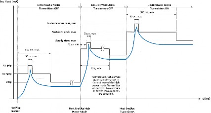
Specification values for maximum instantaneous, sustained and steady state currents at each power class are given in Table 7. The module shall not be affected by the instantaneous variations of the power supply caused by its own current drawing profile during all power transient events.
The module and all pins shall withstand 500V electrostatic discharge based on Human Body Model per JEDEC JESD22-A114-B.
The module shall meet ESD requirements given in EN61000-4-2, criterion B test specification such that when installed in a properly grounded cage and chassis the units are subjected to 15KV air discharges during operation and 8KV direct contact discharges to the case.
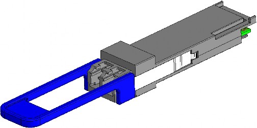
The overall module defined in this clause is illustrated in Figure 9. The module and connector dimensions described in this clause are constant for all applications. The bezel, cage assembly, heat sink can be designed and/or adjusted for the individual application.
A listing of the datums for the various components is contained in Table 8. The alignments of some of the datums are noted. The relationship of the Module, Cage, and Connector relative to the Host Board and Bezel are illustrated in Figure 10 and Figure 11 by the location of the key datums of each of the components. In order to reduce the complexity of the drawings, all dimensions are considered centered unless otherwise specified.
Datums D, K, L, N and T are aligned when assembled
Centerlines of datums AA,C,E,G,M,P and Z are aligned on the same vertical axis
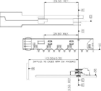
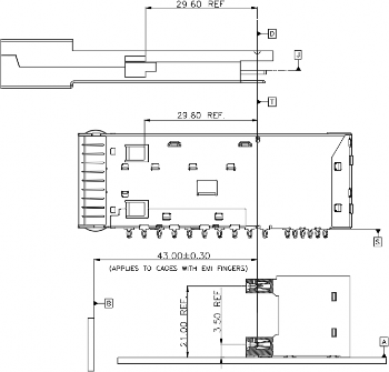
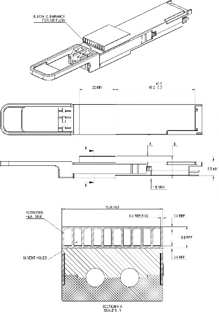
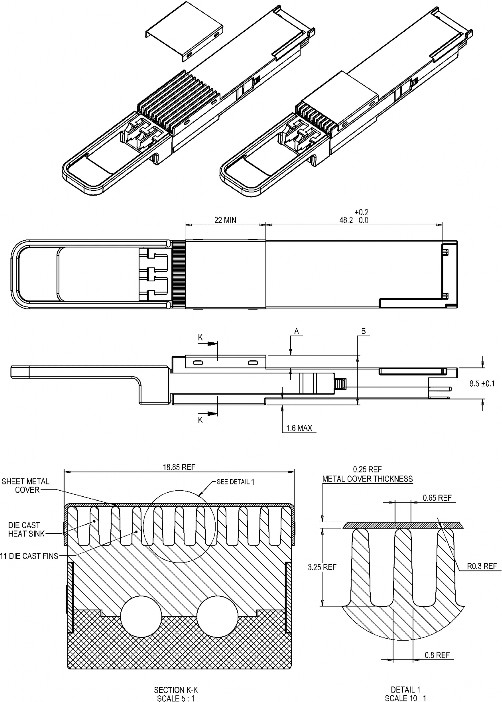
A common mechanical outline is used for all QSFP112 modules. The shell provides a means to self-lock with the cage upon insertion. The package dimensions for the QSFP112 module are defined in Figure 12 and Figure 13. The dimensions that control the size of the module that extends outside of the cage are listed as maximum dimensions per below Note 4 and Note 8 in Figure 12.
NOTES APPLY TO MODULE DRAWING
DIMENSIONS AND TOLERANCING CONFORM TO ASME Y14.5-2009.
ALL DIMENSIONS ARE IN MILLIMETERS.
UNLESS OTHERWISE SPECIFIED, SHARP CORNERS, EDGES, AND BURRS ARE NOT ALLOWED. ROUND OFF ALL EDGES AND CORNERS TO A MINIMUM RADIUS OF 0.2MM.
DIMENSIONS DEFINES ENLARGED SECTION OF TRANSCEIVER THAT EXTENDS OUTSIDE OF CAGE TO ACCOMMODATE MATING PLUG AND ACTUATOR MECHANISM.
SURFACES ON ALL 4 SIDES OF THE 12.4 MIN DIMENSION TO BE CONDUCTIVE FOR CONNECTION TO CHASSIS GROUND.
DIMENSION APPLIES TO LATCH MECHANISM.
DIMENSION APPLIES TO THE LOCATION OF THE EDGE OF THE MODULE BOARD PAD, DATUM H. CONTACTS 21, 22, 36, AND 37 ARE VISIBLE.
DIMENSION TO INCLUDE BAIL TRAVEL.
DIMENSION APPLY TO OPENNINGS IN THE HOUSING.
FEATURE MAY BE LONGER THAN SHOWN.
FLATNESS AND SURFACE ROUGHNESS (Ra) APPLIES FOR INDICATED LENGTH AND MIN WIDTH OF 13MM. SURFACE TO BE THERMALLY CONDUCTIVE. SEE SECTION 5.3.2 TABLE 9 FOR FLATNESS AND ROUGHNESS REQUIREMENS.
HIGH WATTAGE MODULES MAY REQUIRE ADDITIONAL SPACE FOR COOLING.
NO LABEL SHALL BE APPLIED IN THIS AREA FOR TYPE 2/2A/2B. ETCHINGS ARE ALLOWED BUT MUST NOT AFFECT THERMAL PERFORMANCE.
THE LABEL(S) MUST NOT INTERFERE WITH THE MECHANICAL, THERMAL, OR EMI PERFORMANCE AND MUST NOT VIOLATE NOTE 5.
QSFP112 module flatness and roughness are specified to improve module thermal characteristics when used with a riding heat sink. Relaxed specifications are used for lower power modules to reduce cost. The module flatness and roughness specifications apply to the specified heat sink contact area for QSFP112 by Figure 12 and Figure13. Specifications for QSFP112 Module flatness and surface roughness are shown in Table 9. Flatness and roughness specifications applies to both top and bottom surfaces of the modules. Power class 1Cu is dedicated to passive copper cables with a more relaxed flatness of 0.15 mm.
Power Class1 | Module Flatness (mm) | Surface Roughness (Ra, μm) |
1Cu2 | 0.15 | 1.6 |
1 | 0.075 | 1.6 |
2 | 0.075 | 1.6 |
3 | 0.075 | 1.6 |
4 | 0.075 | 1.6 |
5 | 0.075 | 1.6 |
6 | 0.075 | 1.6 |
7 | 0.075 | 1.6 |
8 | 0.050 | 0.8 |
|
QSFP112 power classes are defined in Table 6.
Power class 1Cu maximum power dissipation is the same as power class 1.
The pad definition data is generic for high speed datacom applications such as Fiber Channel, Ethernet and SONET/ATM.
To support 112 Gb/s serial data rates the QSFP112 module paddle card pad dimensions have been modified. See Figure 14 for QSFP112 module updated paddle card pad dimensions, which uses 0.45 mm in width and 1.4mm in length. All other module dimensions, except for the pads, remain the same as the QSFP+/QSFP28 specifications.
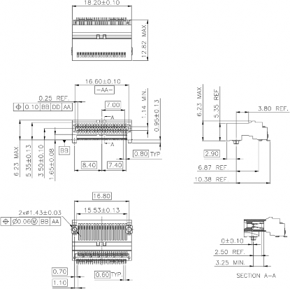
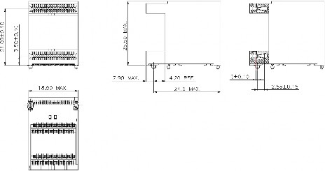
A typical host board mechanical layout of single mount for attaching the QSFP112 Connector and Cage System is shown in Figure 15 , Figure 16, Figure 17, Figure 18 and Figure 19, the connector and the cage can also support belly to belly application of host board. Location of the pattern on the host board is application specific. See Clause 4.6 for details on the location of the pattern relative to the bezel.
QSFP112 module and cage system insertion, extraction, and retentions forces are given in Table 10. QSFP 112 connector and cage retention system are designed to withstand excessive force applied through the module or cable. The general requirement as applied to the values in the table is that no functional damage shall occur to the module, connector or cage.
An exposed feature of the QSFP 112 module (a feature or surface extending outside of the bezel) shall be color coded as follows:
Beige for 850nm Blue for 1310nm White for 1550nm
Each QSFP112 module shall be clearly labeled. The complete labeling need not be visible when the QSFP 112 module is installed. The bottom of the device is the recommended location for the label. Labeling shall include:
Appropriate manufacturer and part number identification Appropriate regulatory compliance labeling
A manufacturing traceability code
The label should also include clear specification of the external port characteristics such as: Optical wavelength
Required fiber characteristics (i.e. MMF/SMF) Operating data rate
Interface standards supported Link length supported Connector Type
The labeling shall not interfere with the mechanical, thermal or EMI features.
Host enclosures that use QSFP112 devices should provide appropriate clearances between the QSFP112 modules to allow insertion and extraction without the use of special tools and a bezel enclosure with sufficient mechanical strength. See Figure 12 for the recommended bezel designs. The recommended host board thickness for belly-to-belly mounting of the assemblies is 2.2mm minimum.
Applications with host boards less than 2.2 mm minimum will require module dimensions of less than
1.6 mm shown with Note 1 of Figure 12.
The front surface of the cage assembly passes through the bezel. If EMI spring fingers are used, they make contact to the inside of the bezel cutouts. If an EMI gasket is used, it makes contact to the inside surface of the bezel. To accept all cage designs, both bezel surfaces must be conductive and connected to chassis ground.
The recommended basic dimension from the bezel centerline to Datum K and Datum L (See Figure 6 and Figure 12) on the Host board is 43.8mm nominal. The total tolerance can be calculated as follows:
+/- tolerance = 1/2 (bezel thickness) + 0.3mm
For example, a bezel thickness of 1.6mm will have a bezel centerline tolerance of +/- 1.1mm.
The dimension of 43.8 +/- 1.1mm would apply from the Centerline of the bezel to Datums K and L. The QSFP112 module insertion slot should be clear of nearby moldings and covers that might block convenient access to the latching mechanisms, the QSFP112 module, or the cables connected to the QSFP112 module.
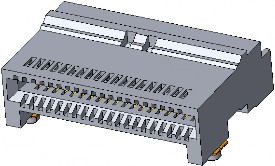
The QSFP112 Connector is a 38-contact, right angle surface mount connector and is shown in Figure
22. The mechanical specification for the connector is shown in Figure 23 and Figure 24.
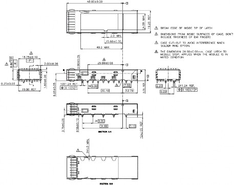
The detailed drawings for the cage assembly and reference type of heatsinks are shown in Figure 26, Figure 28, Figure 29 and Figure 30. The 3D reference view of QSFP112 1x1 and 2x1 cage with heat sink and light pipe are shown in Figure 25 and 27. In Figures 25, 27, 29 and 30, the type of heat sinks illustrated are for reference only with the exception of the heat sink base which touches the QSFP module.
For heat sink applications of single cage, the heat sink must be placed on at least one wall of the cage, where it is in contact with or pressed against the module.
For heat sink applications of QSFP112 stacked cage, a heat sink must be placed in the middle channel of the cage, where the heat sink needs to be in contact with or pressed against the module, and the front, side or rear wall of the cage must be provided with a plurality of heat dissipation holes to provide access to the cooling airflow.
For light pipe applications of QSFP112 single cage light pipe, the light pipe is placed adjacent to at least one wall of the cage and must pass through the exterior, interior or intermediate channels of the cage, where the light pipe guides the indicator light source to an indicator light display.
For light pipe applications of QSFP112 stacked cage light pipe, the light pipe is placed adjacent to at least one wall of the cage and must pass through the exterior, interior or intermediate channels of the cage, where the light pipe guides the indicator light source to an indicator light display.

(The type of heat sink illustrated is for reference only)
.png")
(The types of heat sinks illustrated are for reference only)

(The type of heat sink illustrated is for reference only)

(The type of heat sink illustrated is for reference only)
The QSFP112 Qpath112 connector and cage is a 38-contact connector and cage containing high-speed signal contacts that are ultimately connected to cables and low speed and power contacts that are pressed fit to the PCB. The detailed drawings for the Qpath112 connector and cage are shown in Figure 31, Figure 32, Figure 33 and Figure 34.

The QSFP112 with 4 transmit lanes [Tx1-Tx4] and 4 receive lanes [Rx1-Rx4] allows optical port mapping as shown in Table 11.
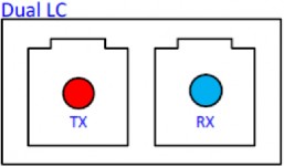
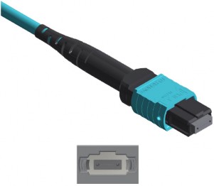
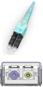
The recommended location and numbering of the optical ports for 3 Media Dependent Interfaces (MDI) are shown in Figure 35. The transmit and receive optical lanes shall occupy the positions depicted in Figure 35 when looking into the MDI receptacle with the connector keyway feature on top. QSFP112 optical MDI examples are shown for a male MPO receptacles (see Figure 36) and a dual LC (see Figure 37).
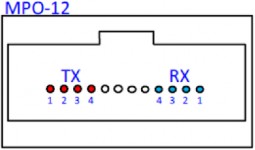
The optical plug and receptacle for the MPO-12 connectors are specified in TIA-604-5 and shown in Figure 36 (MPO-12 Single Row).
Aligned keys are used to ensure alignment between the modules and the patch cords. The optical connector is orientated such that the keying feature of the MPO receptacle is on the top.
Note: Two alignment pins are present in each receptacle.
The Dual LC optical patchcord and module receptacle is specified in TIA-604-10 and shown in Figure 37.
The QSFP112 module shall operate within one or more of the case temperatures ranges defined in Table 12 (a) / Table 12(b). The temperature ranges are applicable between 60m below sea level and 1800m above sea level, (Ref. NEBS GR-63) utilizing the host systems designed airflow.
Class | Case Temperature Range |
Standard | 0 through 70°C |
Extended | -5 through 85°C |
Industrial | -40 through 85°C |
Class | Functional Case Temperature | Case Temperature |
A1 | 15 - 60°C | 25 - 60°C |
A2 | 5 - 60°C | 15 - 60°C |
A3 | 5 - 70°C | 15 - 70°C |
A4 | 5 - 75°C | 15 - 75°C |
QSFP112 is designed to allow for up to 16 adjacent modules, ganged and/or belly-to-belly, with the appropriate thermal design for cooling / airflow. (Ref. NEBS GR-63)
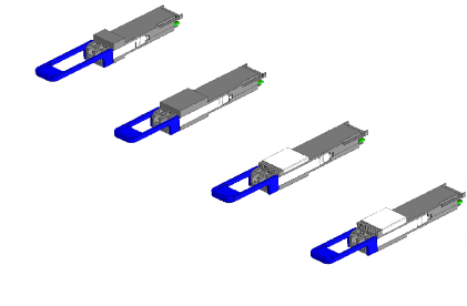
For module dimensions all remain the same as the QSFP+/QSFP28 specifications except for the nose protrusion outside of the faceplate of the equipment, Figure 38 shows the four variants of the QSFP112 modules. Type 1 being consistent with the QSFP28 mechanicals and Type 2 having a longer extension beyond the faceplate that module manufacturers can take advantage of for extra design room internal to the module. Type 2A is a further variant on Type 2 which has an integrated heatsink on the nose of the module to facilitate cooling with an efficient secondary heat transfer path. Type 2B increases the height of the nose heatsink to handle higher module power consumption up to 25W. All module variants are compatible with the common QSFP112 connector and cage designs and can be intermixed in a deployment. The main differences listed below.
Type 1
Type 2
Type 2A
Type 2B
A management interface, as already commonly used in other form factors like QSFP, SFP, is specified in order to enable flexible use of the module by the user. The specification has been changed in order to adopt the use of a multi-channel module. Some timing requirements are critical especially for a multi- channel device, so the interface speed has been increased.
Byte 00h or Byte 128h on Page 00h is used to indicate the use of SFF-8636 or CMIS with 4 host lanes instead of 8 lanes. When a classic QSFP+/QSFP28 module is inserted into a QSFP112 port the host must determine which memory map to use (e.g., SFF-8636 or CMIS) based on the QSFP+ identifier at Byte 00h or Byte 128 Page 00h. The Identifier Value assigned to the module is essential to interpreting the contents of the memory map.
Value | Description of Module |
0Dh | QSFP+ or later with SFF-8636 or SFF-8436 management interface (SFF-8436, SFF-8635, SFF-8665, SFF-8685 et al.) |
1Eh | QSFP+ or later with Common Management Interface Specification (CMIS) |
In some applications, muxing or demuxing may occur in the module. In this specification, all references to lane numbers are based on the electrical connector interface lanes, unless otherwise indicated. In cases where a status or control aspect is applicable only to lanes after muxing or demuxing has occurred, the status or control is intended to apply to all lanes in the mux group, unless otherwise indicated.
Low speed signaling is based on Low Voltage CMOS (LVCMOS) operating at Vcc. Hosts shall use a pull- up resistor connected to a Vcc_host on the TWI SCL (clock) and SDA (Data) signals. Detailed electrical specification is given in Clause 4.1.2. Nomenclature for all registers more than 1 bit long is MSB-LSB.
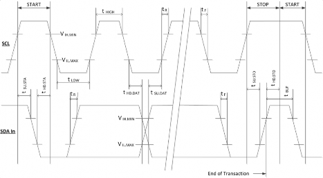
The timing parameters for the TWI to the QSFP112 module memory transaction timings are shown in Figure 39 and specified in Table 14 and is compatible with I2C. The default clock rate is a maximum of 400 kHz with an option to support up to a maximum of 1 MHz. This clause closely follows the QSFP+ SFF-8636 specification but with the addition of Fast Mode+. This specification also defines tBUF timing, tWR timing, tNACK timing, tBPC timing.
The TWI serial interface address of the QSFP112 module is 1010000X (A0h). In order to allow access to multiple QSFP modules on the same TWI serial bus, the QSFP112 pinout includes a ModSelL or module select pin. This pin (which is pulled high, deselected in the module) must be held low by the host to select the module of interest and allow communication over the TWI serial interface. The module must not respond to or accept TWI serial bus instructions unless it is selected.
Before initiating a TWI serial bus communication, the host shall provide setup time on the ModSelL line of all modules on the TWI bus. The host shall not change the ModSelL line of any module until the TWI serial bus communication is complete and the hold time requirement is satisfied.
The module asserts LOW for clock stretch on SCL.
The timing parameters for the TWI to the QSFP112 module are shown in Table 14.
Timing for QSFP112 soft control and status functions are described in Table 15.
Power on is defined as the instant when supply voltages reach and remain at or above the minimum level specified in Table 7.
Measured from low to high SDA edge of the Stop condition of the read transaction.
Rx LOS condition is defined at the optical input by the relevant standard.
Tx Squelch Deassert time is longer than SFF-8679.
Measured from low to high SDA edge of the Stop condition of the write transaction.
Measured from the low to high SDA edge of the Stop condition of the Write transaction until the IntL for the state change Vout:IntL=Vol, unless the module advertises a less than 1 ms duration in which case there is no defined measurement.
Measured from the low to high SDA edge of the Stop condition of the Write transaction until the IntL for
Squelch and disable timings are defined in Table 16.
Serial Clock (SCL): The host supplied SCL input to QSFP112 modules is used to positive-edge clock data into each QSFP112 device and negative-edge clock data out of each device. The SCL line may be pulled low by an QSFP112 module during clock stretching.
Serial Data (SDA): The SDA pin is bi-directional for serial data transfer. This pin is open-drain or open- collector driven and may be wire-ORed with any number of open-drain or open collector devices.
Master/Slave: QSFP112 modules operate only as slave devices. The host must provide a bus master for SCL and initiate all read/write communication.
Device Address: Each QSFP112 is hard wired at the device address A0h. See Clause 7.6 for memory structure within each module.
Multiple Devices per SCL/SDA: While QSFP112 modules are compatible with point-to-point SCL/SDA, they can share a single SCL/SDA bus by using the QSFP112 ModSelL line. See Clause 4.1.1,Clause 4.1.2
, Table 3 for more information.
Clock and Data Transitions: The SDA pin is normally pulled high with an external device. Data on the SDA pin may change only during SCL low time periods. Data changes during SCL high periods indicate a START or STOP condition. All addresses and data words are serially transmitted to and from the QSFP112 in 8-bit words.
Every byte on the SDA line must be 8-bits long. Data is transferred with the most significant bit (MSB) first.
START Condition: A high-to-low transition of SDA with SCL high is a START condition, which must precede any other command.
STOP Condition: A low-to-high transition of SDA with SCL high is a STOP condition.
Acknowledge: After sending each 8-bit word, the transmitter releases the SDA line for one bit time, during which the receiver is allowed to pull SDA low (zero) to acknowledge (ACK) that it has received each word. Device address bytes and write data bytes initiated by the host shall be acknowledged by QSFP112 modules.
Read data bytes transmitted by QSFP112 modules shall be acknowledged by the host for all but the final byte read, for which the host shall respond with a STOP instead of an ACK.
Memory (Management Interface) Reset: After an interruption in protocol, power loss or system reset the QSFP112 management interface can be reset. Memory reset is intended only to reset the QSFP112 module management interface (to correct a hung bus). No other module functionality is implied.
Clock up to 9 cycles.
Look for SDA high in each cycle while SCL is high.
Create a START condition as SDA is high
Device Addressing: QSFP112 devices require an 8-bit device address word following a start condition to enable a read or write operation. The device address word consists of a mandatory sequence for the first seven most significant bits in Figure 40. This is common to all QSFP112 devices.
The eighth bit of the device address is the read/write operating select bit. A read operation is initiated if this bit is set high and a write operation is initiated if this bit is set low. Upon compare of the device address (with ModSelL in the low state) the QSFP112 module shall output a zero (ACK) on the SDA line to acknowledge the address.
QSFP112 devices maintain an internal data word address counter containing the last address accessed during the latest read or write operation, incremented by one. The address counter is incremented whenever a data word is received or sent by the module. This address stays valid between operations as long as QSFP112 power is maintained. The address “roll over” during read and writes operations is from the last byte of the 128-byte memory page to the first byte of the same page.
A current address read operation requires only the device address read word (10100001) be sent, see Figure 41. Once acknowledged by the QSFP112, the current address data word is serially clocked out. The host does not respond with an acknowledge, but does generate a STOP condition once the data word is read.
A random read operation requires a “dummy” write operation to load in the target byte address as shown in Figure 42. This is accomplished by the following sequence: The target 8-bit data word address is sent following the device address write word (10100000) and acknowledged by the QSFP112. The host then generates another START condition (aborting the dummy write without incrementing the counter) and a current address read by sending a device read address (10100001). The QSFP112 acknowledges the device address and serially clocks out the requested data word. The host does not respond with an acknowledge, but does generate a STOP condition once the data word is read.
Sequential reads are initiated by either a current address read (Figure 43) or a random address read (Figure 44). To specify a sequential read, the host responds with an acknowledge (instead of a STOP) after each data word. As long as the QSFP112 receives an acknowledge, it shall serially clock out sequential data words. The sequence is terminated when the host responds with a NACK and a STOP instead of an acknowledge.
A write operation requires an 8-bit data word address following the device address write word (10100000) and acknowledgement, see Figure 45. Upon receipt of this address, the QSFP112 shall again respond with a zero (ACK) to acknowledge and then clock in the first 8-bit data word. Following the receipt of the 8-bit data word, the QSFP112 shall output a zero (ACK) and the host master must terminate the write sequence with a STOP condition for the write cycle to begin. If a START condition is sent in place of a STOP condition (i.e. a repeated START per the TWI specification) the write is aborted and the data received during that operation is discarded. Upon receipt of the proper STOP condition, the QSFP112 enters an internally timed write cycle, tWR, to internal memory. The QSFP112 disables it is management interface input during this write cycle and shall not respond or acknowledge subsequent commands until the write is complete. Note that TWI “Combined Format” using repeated START conditions is not supported on QSFP112 write commands.
QSFP shall support up to a 4 sequential byte write without repeatedly sending QSFP112 address and memory address information as shown in Figure 46. A “sequential” write is initiated the same way as a single byte write, but the host master does not send a stop condition after the first word is clocked in. Instead, after the QSFP112 acknowledges receipt of the first data word, the host can transmit up to three more data words. The QSFP112 shall send an acknowledge after each data word received. The host must terminate the sequential write sequence with a STOP condition or the write operation shall be aborted and data discarded. Note that TWI “combined format” using repeated START conditions is not supported on QSFP112 write commands.
Once the QSFP112 internally timed write cycle has begun (and inputs are being ignored on the bus) acknowledge polling can be used to determine when the write operation is complete. This involves sending a START condition followed by the device address word. Only if the internal write cycle is complete shall the QSFP112 respond with an acknowledge to subsequent commands, indicating read or write operations can continue.
QSFP112 management interface, as already commonly used in other form factors like QSFP and SFP, is specified in order to enable flexible use of the module by the user. The memory map for QSFP112 is found in “Common Management Interface Specification (CMIS 5.0) or later”.
Several informative designs examples of higher power Type 2A and 2B QSFP112 with integrated nose heat sinks are shown in Figure 47, Figure 48, and Figure 49.
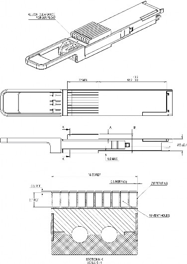
Thermal design is system dependent; however, systems seeking to maximize the benefit of the external heat sink of Type 2A and 2B modules should consider minimizing bypass of airflow through the external heat sink. Type 2A and 2B modules have a heat sink on the nose of the module. The QSFP112 type 2B modules are taller and can only be used in special stack cages as the ports on a thermal enhanced stacked QSFP112 cage are separated by 1.7mm more than normal QSFP112 stack cages. However, a Type 2A module can be used in all applications.
Type 2A and Type 2B extruded heat sink examples are shown in Figure 47. Type 2A and Type 2B die
cast heat sinks with metal cover examples are shown in Figure 48. Type 2A and Type 2B zipper fin heat sink examples are shown in Figure 49. Dimensions A, B for Type 2A and 2B heat sinks in Figure 47, Figure 48, and Figure 49 are given in Table 17. All dimensions shall have dimension tolerance of +/-0.1 mm.
Dimensions | Module Type 2A | Module Type 2B |
A (max) | 3.4 mm | 5.1 mm |
B (REF) | 13.5 mm | 15.2 mm |