
Part Number: QSFP-40G-ZR4-FL QSFP-40G-ZR4-FL-EXT QSFP-40G-ZR4-FL-IND
Form Factor: QSFP
TX Wavelength: 1296,1300, 1305, 1309nm
Reach: 80km
Cable Type: SMF
Rate Category: 40GBase
Interface Type: ZR4
DDM: Yes
Connector Type: Dual-LC
Juniper Compatible QSFP-40G-ZR4-FL Features
4 lanes MUX/DEMUX design
Integrated LAN WDM TOSA / ROSA
Up to 11.2Gbps per channel bandwidth
Aggregate bandwidth of > 40Gbps
Duplex LC connector
Compliant with 40G Ethernet IEEE802.3ba and 40GBASE-ZR4
QSFP MSA compliant
APD photo-detector
Up to 80 km transmission
Compliant with QDR/DDR Infiniband data rates
Single +3.3V power supply operating
Built-in digital diagnostic functions
RoHS compliant
Operating Case Temperature
Standard: 0°C to +70 °C
Extended -5°C to +85 °C
Industrial -40°C to +85 °C
Juniper Compatible QSFP-40G-ZR4-FL Applications
Rack to rack
Data centers Switches and Routers
Metro networks
Switches and Routers
40G BASE-ZR4 Lite
Juniper Compatible QSFP-40G-ZR4-FL General Description
This QSFP-40G-ZR4-FL is a transceiver module designed for 80km optical communication applications. The design is compliant to 40GBASE-ER4 of the IEEE P802.3ba standard. The module converts 4 inputs channels of 10Gb/s electrical data to 4 CWDM optical signals, and multiplexes them into a single channel for 40Gb/s optical transmission. Reversely, on the receiver side, the module optically de-multiplexes a 40Gb/s input into 4 CWDM channels signals, and converts them to 4 channel output electrical data.
The central wavelengths of the 4 LANWDM channels are 1296 nm, 1300 nm, 1305 nm and 1309 nm as members of the
LAN WDM wavelength grid defined in ITU-T G694.2. It contains a duplex LC connector for the optical interface and a 38- pin connector for the electrical interface. To minimize the optical dispersion in the long-haul system, single-mode fiber (SMF) has to be applied in this module.
The product is designed with form factor, optical/electrical connection, and digital diagnostic interface according to the QSFP Multi-Source Agreement (MSA). It has been designed to meet the harshest external operating conditions including temperature, humidity and EMI interference.
The module operates from a single +3.3V power supply and LVCMOS/LVTTL global control signals such as Module Present, Reset, Interrupt and Low Power Mode are available with the modules. A 2-wire serial interface is available to send and receive more complex control signals and to obtain digital diagnostic information. Individual channels can be addressed and unused channels can be shut down for maximum design flexibility.
The QSFP-40G-ZR4-FL is designed with form factor, optical/electrical connection and digital diagnostic interface according to the QSFP Multi-Source Agreement (MSA). It has been designed to meet the harshest external operating conditions including temperature, humidity and EMI interference. The module offers very high functionality and feature integration, accessible via a two-wire serial interface.
.
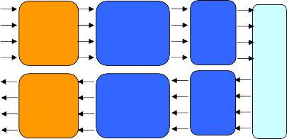
DFB Driver Array (4ch)
4-wavelength
DFB
laser
Optical MUX
Array (4ch)
APD
Array (4ch)
APD
Array (4ch)
Optical DeMUX
TX3 TX2 TX1 TX0
RX3 RX2 RX1 RX0
Dual-LC Connector
![]()
Single Mode Fiber
![]()
Pin Assignment and Description

Diagram of Host Board Connector Block Pin Numbers and Name
Pin | Logic | Symbol | Description | Plug Sequence |
1 | GND | Ground | 1 | |
2 | CML-I | Tx2n | Transmitter Inverted Data Input | |
3 | CML-I | Tx2p | Transmitter Non-Inverted Data output | |
4 | GND | Ground | 1 | |
5 | CML-I | Tx4n | Transmitter Inverted Data Output | |
6 | CML-I | Tx4p | Transmitter Non-Inverted Data Output | |
7 | GND | Ground | 1 | |
8 | LVTTL-I | ModSelL | Module Select | |
9 | LVTTL-I | ResetL | Module Reset | |
10 | VccRx | +3.3V Power Supply Receiver | 2 | |
11 | LVCMOS- I/O | SCL | 2-Wire Serial Interface Clock | |
12 | LVCMOS- I/O | SDA | 2-Wire Serial Interface Data | |
13 | GND | Ground | 1 | |
14 | CML-O | Rx3p | Receiver Inverted Data Output | |
15 | CML-O | Rx3n | Receiver Non-Inverted Data Output | |
16 | GND | Ground | 1 | |
17 | CML-O | Rx1p | Receiver Inverted Data Output | |
18 | CML-O | Rx1n | Receiver Non-Inverted Data Output | |
19 | GND | Ground | 1 | |
20 | GND | Ground | 1 | |
21 | CML-O | Rx2n | Receiver Inverted Data Output | |
22 | CML-O | Rx2p | Receiver Non-Inverted Data Output | |
23 | GND | Ground | 1 | |
24 | CML-O | Rx4n | Receiver Inverted Data Output | |
25 | CML-O | Rx4p | Receiver Non-Inverted Data Output | |
26 | GND | Ground | 1 | |
27 | LVTTL-O | ModPrsL | Module Present | |
28 | LVTTL-O | IntL | Interrupt | |
29 | VccTx | +3.3V Power Supply Transmitter | 2 | |
30 | Vcc1 | +3.3V Power Supply | 2 | |
31 | LVTTL-I | LPMode | Low Power Mode |
32 | GND | Ground | 1 | |
33 | CML-I | Tx3p | Transmitter Inverted Data Output | |
34 | CML-I | Tx3n | Transmitter Non-Inverted Data Output | |
35 | GND | Ground | 1 | |
36 | CML-I | Tx1p | Transmitter Inverted Data Output | |
37 | CML-I | Tx1n | Transmitter Non-Inverted Data Output | |
38 | GND | Ground | 1 |
GND is the symbol for single and supply(power) common for QSFP modules, All are common within the QSFP module and all module voltages are referenced to this potential otherwise noted. Connect these directly to the host board signal common ground plane. Laser output disabled on TDIS >2.0V or open, enabled on TDIS <0.8V.
VccRx, Vcc1 and VccTx are the receiver and transmitter power suppliers and shall be applied concurrently. Recommended host board power supply filtering is shown below. VccRx, Vcc1 and VccTx may be internally connected within the QSFP transceiver module in any combination. The connector pins are each rated for maximum current of 500mA.
It has to be noted that the operation in excess of any individual absolute maximum ratings might cause permanent damage to this module.
Parameter | Symbol | Min | Max | Units | Notes |
Storage Temperature | TS | -40 | 85 | degC | |
Operating Case Temperature - Commercial | TOP | 0 | 70 | degC | |
Operating Case Temperature - Industrial | TOP | -40 | 85 | degC | |
Power Supply Voltage | VCC T, R | -0.5 | 5 | V | |
Relative Humidity (non-condensation) | RH | 0 | 85 | % |
Recommended Operating Conditions and Power Supply Requirements
Parameter | Symbol | Min | Typical | Max | Units | Notes |
Case Temperature | Tc | 0 | 70 | ℃ | ||
Supply Voltage | VCC T, R | +3.13 | 3.3 | 3.47 | V | |
Supply Current | ICC | 1000 | mA | |||
Power Dissipation | PD | 3.5 | W |
Electrical Characteristics (TOP = 0 to 70 °C, VCC = 3.13 to 3.47 Volts)
Parameter | Test Point | Min | Typical | Max | Units | Notes |
Data Rate per Channel | - | 10.3125 | 11.2 | Gbps | ||
Power Consumption | - | 2.5 | 5 | W | ||
Supply Current | Icc | 0.75 | 1.3 | A | ||
Control I/O Voltage-High | VIH | 2.0 | Vcc | V | ||
Control I/O Voltage-Low | VIL | 0 | 0.7 | V | ||
Inter-Channel Skew | TSK | 150 | Ps | |||
RESETL Duration | 10 | Us | ||||
RESETL De-assert time | 100 | ms | ||||
Transmitter (each Lane) | ||||||
Single Ended Output Voltage Tolerance | 0.3 | 4 | V | 1 | ||
Common mode Voltage Tolerance | 15 | mV | ||||
Transmit Input Diff Voltage | VI | 150 | 1200 | mV | ||
Transmit Input Diff Impedance | ZIN | 85 | 100 | 115 | ||
Data Dependent Input Jitter | DDJ | 0.3 | UI | |||
Receiver (each Lane) | ||||||
Single Ended Output Voltage Tolerance | 0.3 | 4 | V | |||
Rx Output Diff Voltage | Vo | 370 | 600 | 950 | mV | |
Rx Output Rise and Fall Voltage | Tr/Tf | 35 | ps | 1 | ||
Total Jitter | TJ | 0.3 | UI | |||
Notes:
20%~80%
Optical Characteristics (TOP = 0 to 70 °C, VCC = 3.0 to 3.6 Volts)
Parameter | Symbol | Min | Typical | Max | Units | Notes |
Transmitter | ||||||
Wavelength Assignment | L0 | 1294.53 | 1295.56 | 1296.59 | nm | |
L1 | 1299.02 | 1300.05 | 1301.09 | nm | ||
L2 | 1303.54 | 1304.58 | 1305.63 | nm | ||
L3 | 1308.09 | 1309.14 | 1310.19 | nm | ||
Side-mode Suppression Ratio | SMSR | 30 | - | - | dB | |
Total Average Launch Power | PT | - | 10.5 | dBm | ||
Average Launch Power, each Lane | +4 | - | 7 | dBm | ||
Transmit OMA per Lane | TxOMA | 0.3 | 5.0 | dBm | ||
Difference in launch power between any two lanes (OMA) | 4.7 | dBm | ||||
Transmitter Dispersion Penalty each Lane | TDP | 2.6 | dB | |||
Extinction Ratio | ER | 5.5 | 6.5 | dB | ||
Transmitter Eye Mask Definition {X1, X2, X3, Y1, Y2, Y3} | {0.25, 0.4, 0.45, 0.25, 0.28, 0.4} | |||||
Optical Return Loss Tolerance | - | - | 20 | dB | ||
Average Launch Power OFF Transmitter, each Lane | Poff | -30 | dBm | |||
Relative Intensity Noise | Rin | -128 | dB/HZ | 1 | ||
Optical Return Loss Tolerance | - | - | 12 | dB | ||
Receiver | ||||||
Damage Threshold | THd | 0 | dBm | 1 | ||
Average Power at Receiver Input, each Lane | R | -24 | -6 | dBm | ||
Receive Electrical 3 dB upper Cut off Frequency, each Lane | 12.3 | GHz | ||||
RSSI Accuracy | -2 | 2 | dB | |||
Receiver Reflectance | Rrx | -26 | dB | |||
Receiver Power (OMA), each Lane | - | - | -4 | dBm | ||
Receive Electrical 3 dB upper Cutoff Frequency, each Lane | 12.3 | GHz | ||||
LOS De-Assert | LOSD | -25 | dBm | |||
LOS Assert | LOSA | -35 | dBm | |||
LOS Hysteresis | LOSH | 0.5 | dB | |||
Notes:
1. 12dB Reflection
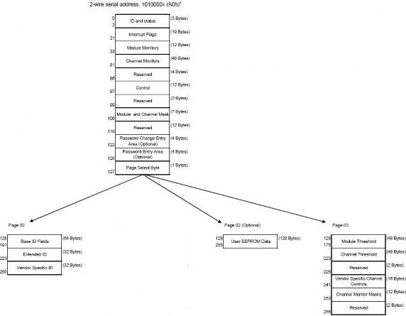
Digital diagnostics monitoring function is available on all QSFP+ ZR4. A 2-wire serial interface provides user to contact with module. The structure of the memory is shown in flowing. The memory space is arranged into a lower, single page, address space of 128 bytes and multiple upper address space pages. This structure permits timely access to addresses in the lower page, such as Interrupt Flags and Monitors. Less time critical time entries, such as serial ID information and threshold settings, are available with the Page Select function. The interface address used is A0xh and is mainly used for time critical data like interrupt handling in order to enable a one-time-read for all data related to an interrupt situation. After an interrupt, IntL has been asserted, the host can read out the flag field to determine the affected channel and type of flag.
EEPROM Serial ID Memory Contents (A0h)
Data Address | Length (Byte) | Name of Length | Description and Contents |
Base ID Fields | |||
128 | 1 | Identifier | Identifier Type of serial Module(D=QSFP+) |
129 | 1 | Ext. Identifier | Extended Identifier of Serial Module(90=2.5W) |
130 | 1 | Connector | Code of connector type(7=LC) |
131-138 | 8 | Specification compliance | Code for electronic compatibility or optical compatibility(40GBASE- LR4) |
139 | 1 | Encoding | Code for serial encoding algorithm(5=64B66B) |
140 | 1 | BR, Nominal | Nominal bit rate, units of 100 MBits/s(6C=108) |
141 | 1 | Extended rateselect Compliance | Tags for extended rate select compliance |
142 | 1 | Length(SMF) | Link length supported for SMF fiber in km (28=80km) |
143 | 1 | Length(OM3 50um) | Link length supported for EBW 50/125um fiber(OM3), units of 2m |
144 | 1 | Length(OM2 50um) | Link length supported for 50/125um fiber(OM2), units of 1m |
145 | 1 | Length(OM1 62.5um) | Link length supported for 62.5/125um fiber (OM1), units of 1m |
146 | 1 | Length(Copper) | Link length of copper or active cable, unites of 1m Link length supported for 50/125um fiber (OM4), units of 2m when Byte 147 declares 850nm VCSEL as defined in Table 37 |
147 | 1 | Device tech | Device technology |
148-163 | 16 | Vendor name | QSFP+ vendor name: TIBTRONIX (ASCII) |
164 | 1 | Extended Module | Extended Module codes for InfiniBand |
165-167 | 3 | Vendor OUI | QSFP+ vendor IEEE company ID(000840) |
168-183 | 16 | Vendor PN | Part number: TQPLFG80D (ASCII) |
184-185 | 2 | Vendor rev | Revision level for part number provided by vendor (ASCII) (X1) |
186-187 | 2 | Wave length or Copper cable Attenuation | Nominal laser wavelength (wavelength=value/20 in nm) or copper cable attenuation in dB at 2.5GHz (Adrs 186) and 5.0GHz (Adrs 187) (65A4=1301) |
188-189 | 2 | Wavelength tolerance | Guaranteed range of laser wavelength(+/- value) from nominal wavelength. (wavelength Tol.=value/200 in nm) (1C84=36.5) |
190 | 1 | Max case temp. | Maxinum case temperature in degrees C (70) |
191 | 1 | CC_BASE | Check code for base ID fields (addresses 128-190) |
Extended ID fields | |||
192-195 | 4 | Options | Rate Select, TX Disable, Tx Fault, LOS, Warning indicators for: Temperature, VCC, RX, power, TX Bias |
196-211 | 16 | Vendor SN | Serial number provided by vendor (ASCII) |
212-219 | 8 | Date Code | Vendor's manufacturering date code |
220 | 1 | Diagnostic Monitoring Type | Indicates which types of diagnostic monitoring are implemented (if any) in the Module. Bit 1, 0 Reserved (8=Average Power) |
221 | 1 | Enhanced Options | Indicates which optional enhanced features are implemented in the Module. |
221 | 1 | Reserveed | |
223 | 1 | CC_EXT | Check code for the Extended ID Fields (addresses 192-222) |
Vendor Specific ID Fields | |||
224-255 | 32 | Vendor Specific EEPROM | |
Timing for Soft Control and Status Functions
Parameter | Symbol | Max | Unit | Conditions |
Initialization Time | t_init | 2000 | ms | Time from power on1, hot plug or rising edge of Reset until the module is fully functional2 |
Reset Init Assert Time | t_reset_init | 2 | μs | A Reset is generated by a low level longer than the minimum reset pulse time present on the ResetL pin. |
Serial Bus Hardware Ready Time | t_serial | 2000 | ms | Time from power on1 until module responds to data transmission over the 2-wire serial bus |
Monitor Data Ready Time | t_data | 2000 | ms | Time from power on1 to data not ready, bit 0 of Byte 2, deasserted and IntL asserted |
Reset Assert Time | t_reset | 2000 | ms | Time from rising edge on the ResetL pin until the module is fully functional2 |
LPMode Assert Time | ton_LPMode | 100 | μs | Time from assertion of LPMode (Vin:LPMode =Vih) until module power consumption enters lower Power Level |
IntL Assert Time | ton_IntL | 200 | ms | Time from occurrence of condition triggering IntL until Vout:IntL = Vol |
IntL Deassert Time | toff_IntL | 500 | μs | toff_IntL 500 μs Time from clear on read3 operation of associated flag until Vout:IntL = Voh. This includes deassert times for Rx LOS, Tx Fault and other flag bits. |
Rx LOS Assert Time | ton_los | 100 | ms | Time from Rx LOS state to Rx LOS bit set and IntL asserted |
Flag Assert Time | ton_flag | 200 | ms | Time from occurrence of condition triggering flag to associated flag bit set and IntL asserted |
Mask Assert Time | ton_mask | 100 | ms | Time from mask bit set4 until associated IntL assertion is inhibited |
Mask De-assert Time | toff_mask | 100 | ms | Time from mask bit cleared4 until associated IntlL operation resumes |
ModSelL Assert Time | ton_ModSelL | 100 | μs | Time from assertion of ModSelL until module responds to data transmission over the 2-wire serial bus |
ModSelL Deassert Time | toff_ModSelL | 100 | μs | Time from deassertion of ModSelL until the module does not respond to data transmission over the 2-wire serial bus |
Power_over-ride or Power-set Assert Time | ton_Pdown | 100 | ms | Time from P_Down bit set 4 until module power consumption enters lower Power Level |
Power_over-ride or Power-set De- assert Time | toff_Pdown | 300 | ms | Time from P_Down bit cleared4 until the module is fully functional3 |
Power on is defined as the instant when supply voltages reach and remain at or above the minimum specified value.
Fully functional is defined as IntL asserted due to data not ready bit, bit 0 byte 2 de-asserted.
Measured from falling clock edge after stop bit of read transaction.
Measured from falling clock edge after stop bit of write transaction.


This transceiver is specified as ESD threshold 1kV for high speed data pins and 2kV for all other electrical input pins, tested per MIL-STD-883, Method 3015.4 /JESD22-A114-A (HBM). However, normal ESD precautions are still required during the handling of this module. This transceiver is shipped in ESD protective packaging. It should be removed from the packaging and handled only in an ESD protected environment
This is a Class 1 Laser Product according to EN 60825-1:2014. This product complies with 21 CFR 1040.10 and 1040.11 except for deviations pursuant to Laser Notice No. 50, dated (June 24, 2007).
Caution: Use of controls or adjustments or performance of procedures other than those specified herein may result in hazardous radiation exposure.
The following U.S. patents are licensed by Finisar to FluxLight, Inc.:
U.S. Patent Nos: 7,184,668, 7,079,775, 6,957,021, 7,058,310, 6,952,531, 7,162,160, 7,050,720