 Fiber Optic Transceiver")
Juniper Compatible QSFP-100G-LX4-J-FL Quick Spec:
Part Number: QSFP-100G-LX4-J-FL QSFP-100G-LX4-J-EXT-FL QSFP-100G-LX4-J-IND-FL
Form Factor: QSFP28
TX Wavelength: LX4
Reach: 2km
Cable Type: SMF/MMF
Rate Category: 100GBase
Interface Type: LX4
DDM: Yes
Connector Type: Dual-LC
Juniper Compatible QSFP-100G-LX4-J-FL Features:
Hot pluggable QSFP28 MSA form factor
Aggregate bit rate: 103.125 Gbps
Up to 2km reach for G.652 SMF
Up to 100m for OM3 (MMF)
Single +3.3V power supply
Transmitter: uncooled 4x25.78 Gbps
Receiver: 4x25 Gbps PIN ROSA
4x25G Electrical Serial Interface
Maximum power consumption 3.5W
RoHS-6 compliant (lead-free)
Duplex LC receptacle
I2C interface with integrated Digital Diagnostic Monitoring
Operating Case Temperature
Standard: 0°C to +70 °C
Extended -5°C to +85 °C
Industrial -40°C to +85 °C
Juniper Compatible QSFP-100G-LX4-J-FL Applications:
100G Ethernet
Juniper Compatible QSFP-100G-LX4-J-FL Overview
The QSFP28-100GBASE-LX4 is designed for use in 100 Gigabit Ethernet links over single-mode fiber and multi-mode fiber. They are compliant with the QSFP28 MSA and IEEE 802.3ba 100GBASE-LX4.Module-level digital diagnostic
functions are available via an I2C interface, as specified by the QSFP28 MSA. The optical transceiver is compliant per the RoHS Directive 2011/6
Specification:
Absolute Maximum Ratings
The operation in excess of any absolute maximum ratings might cause permanent damage to this module.
Parameter | Symbol | Min | Max | Unit |
Storage Temperature | Ts | -40 | +85 | °C |
Operating Case Temp (Standard) | TOP | 0 | 70 | °C |
Operating Case Temp (Industrial) | TOP | -40 | 85 | °C |
Power Supply Voltage | Vcc | -0.5 | 3.6 | V |
Relative Humidity (non- condensation) | RH | 5 | 95 | % |
Signal Input Voltage | -0.3 | Vcc+0.3 | V | |
Receiver Damage Threshold | +3.4 | dBm |
Electrical Characteristics
The following electrical characteristics are defined over the Recommended Operating Environment unless otherwise specified
Parameter | Symbol | Min | Typ | Max | Unit | Notes |
Supply Voltage | Vcc | 3.15 | 3.45 | V | ||
Supply Current | ICC | 1000 | mA | |||
Input different impedance | Rin | 90 | 100 | 110 | Ω | 2 |
Single ended data input swing | Vin, pp | 120 | 820 | mV | ||
Transmitter Disable Voltage | VDIS | 2 | VCC | V | 3 | |
Transmitter Enable Voltage | VEN | 0 | 0.8 | V | ||
Output different impedance | Rout | 90 | 100 | 110 | Ω | 2 |
Single ended data output swing | Vout, pp | 340 | 850 | mV | 4 | |
LOS Asserted | VLOSA | 2 | VCCHOST | V | 5 | |
LOS De-asserted | VLOSD | 0 | 0.8 | V | 5 | |
Power Supply Rejection | PSR | 50 | mVpp |
1.Maximum total power value is specified across the full temperature and voltage range. 2.Connected directly to TX data input pins. AC coupled thereafter.
Or open circuit.
Into 100Ωdifferential termination.
LossOf Signal is LVTTL. Logic “0” indicates normal operation; logic “1” indicates no signal detected.
Optical Characteristics
Parameter | Symbol | Min | Typ | Max | Unit |
Lane Wavelength | L0 | 1264.5 | 1270 | 1277.5 | nm |
L1 | 1284.5 | 1290 | 1297.5 | ||
L2 | 1304.5 | 1310 | 1317.5 | ||
L3 | 1324.5 | 1330 | 1337.5 |
Optical Characteristics-Transmitter
Parameter | Symbol | Min | Typ | Max | Unit | Notes |
Total Average Launch Power for SMF | POUT | 8.3 | dBm | |||
Total Average Launch Power for MMF | 9.5 | dBm | ||||
Average Output Power per lane for SMF | Pave | -7.0 | 2.3 | dBm | ||
Average Output Power per lane for MMF | -5.0 | 3.5 | dBm | |||
Transmit OMA per Lane for SMF | TxOMA | -6.0 | 3.5 | dBm | ||
Transmit OMA per Lane for MMF | -4.0 | 4.5 | dBm | |||
Extinction Ratio | ER | 3.5 | dB | |||
Sidemode Suppression ratio | SMSR | 30 | dB | |||
Transmitter and Dispersion Penalty | TDP | 2.6 | dB | |||
Transmitter OFF Output Power | POff | -30 | dBm | |||
Transmitter eye mask definition {X1, X2, X3, Y1, Y2, Y3} | {0.31, 0.40, 0.45, 0.34, 0.38, 0.4} | |||||
Optical Characteristics-Receiver
Parameter | Symbol | Min | Typ | Max | Unit | Notes |
Rx Sensitivity (OMA) per lane for SMF | RSENS1 | -8.6 | dBm | |||
Rx Sensitivity (OMA) per lane for MMF | -8.6 | dBm | ||||
Input Saturation Power (Overload) for SMF | PSAT | +2.3 | dBm | |||
Input Saturation Power (Overload) for MMF | +3.5 | |||||
Receiver Reflectance | Rfl | -26 | dBm | |||
Loss of Signal Assert | PA | -30 | dBm | |||
Loss of Signal De-assert | PD | -12.5 | dBm | |||
LOS Hysteresis | PD - PA | 0.5 | 6 | dB |
Block Diagram of Transceiver

Digital Diagnostic Functions
The following digital diagnostic characteristics are defined over the normal operating conditions unless otherwise specified.
Parameter | Symbol | Min | Max | Unit | Notes |
Temperature monitor absolute error | DMI_Temp | -5 | 5 | ℃ | |
Supply voltage monitor absolute error | DMI_VCC | -0.1 | 0.1 | V | |
Channel RX power monitor absolute error | DMI_RX_Ch | -3 | 3 | dB | |
Channel Bias current monitor | DMI_Ibias_Ch | -10% | 10% | mA | |
Channel TX power monitor absolut error | DMI_TX_Ch | -3 | 3 | dB |
Mechanical Dimensions
Units: nm

PIN Assignment and Function Definitions
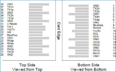
PIN Definition
PIN | Signal Name | Description |
1 | GND | Ground (1) |
2 | Tx2n | CML-I Transmitter 2 Inverted Data Input |
3 | Tx2p | CML-I Transmitter 2 Non-Inverted Data Input |
4 | GND | Ground (1) |
5 | Tx4n | CML-I Transmitter 4 Inverted Data Input |
6 | Tx4p | CML-I Transmitter 4 Non-Inverted Data Input |
7 | GND | Ground (1) |
8 | ModSelL | LVTLL-I Module Select |
9 | ResetL | LVTLL-I Module Reset |
10 | VCCRx | +3.3V Power Supply Receiver (2) |
11 | SCL | LVCMOS-I/O 2-Wire Serial Interface Clock |
12 | SDA | LVCMOS-I/O 2-Wire Serial Interface Data |
13 | GND | Ground (1) |
14 | Rx3p | CML-O Receiver 3 Non-Inverted Data Output |
15 | Rx3n | CML-O Receiver 3 Inverted Data Output |
16 | GND | Ground (1) |
17 | Rx1p | CML-O Receiver 1 Non-Inverted Data Output |
18 | Rx1n | CML-O Receiver 1 Inverted Data Output |
19 | GND | Ground (1) |
20 | GND | Ground (1) |
21 | Rx2n | CML-O Receiver 2 Inverted Data Output |
22 | Rx2p | CML-O Receiver 2 Non-Inverted Data Output |
23 | GND | Ground (1) |
24 | Rx4n | CML-O Receiver 4 Inverted Data Output |
25 | Rx4p | CML-O Receiver 4 Non-Inverted Data Output |
26 | GND | Ground (1) |
27 | ModPrsL | Module Present |
28 | IntL | Interrupt |
29 | VCCTx | +3.3V Power Supply Transmitter (2) |
30 | VCC1 | +3.3V Power Supply |
31 | LPMode | LVTLL-I Low Power Mode |
32 | GND | Ground (1) |
33 | Tx3p | CML-I Transmitter 3 Non-Inverted Data Input |
34 | Tx3n | CML-I Transmitter 3 Inverted Data Input |
35 | GND | Ground (1) |
36 | Tx1p | CML-I Transmitter 1 Non-Inverted Data Input |
37 | Tx1n | CML-I Transmitter 1 Inverted Data Input |
38 | GND | Ground (1) |
Notes:
All Ground (GND) are common within the QSFP+ module and all module voltages are referenced to this potential unless noted otherwise. Connect these directly to the host board signal common ground plane.
VccRx, Vcc1 and VccTx are the receiving and transmission power suppliers and shall be applied concurrently. The connector pins are each rated for a maximum current of 500mA.
ESD
This transceiver is specified as ESD threshold 1kV for SFI pins and 2kV for all other electrical input pins, tested per MIL- STD-883, Method 3015.4 /JESD22-A114-A (HBM). However, normal ESD precautions are still required during the handling of this module. This transceiver is shipped in ESD protective packaging. It should be removed from the packaging and handled only in an ESD protected environment.
Laser Safety
This is a Class 1 Laser Product according to IEC 60825-1:2007. This product complies with 21 CFR 1040.10 and 1040.11 except for deviations pursuant to Laser Notice No. 50, dated (June 24, 2007).
Licensing
The following U.S. patents are licensed by Finisar to FluxLight, Inc.:
U.S. Patent Nos: 7,184,668, 7,079,775, 6,957,021, 7,058,310, 6,952,531, 7,162,160, 7,050,720