Quick Spec:
Part Number: QDD-400G-ZR4-FL QDD-400G-ZR4-EXT-FL QDD-400G-ZR4-IND-FL
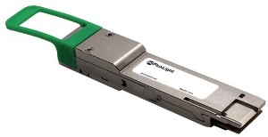
Form Factor: QSFP-DD
TX Wavelength: 1310nm
Reach: 80km
Cable Type: SMF
Rate Category: 400GBase
Interface Type: ZR4
DDM: Yes
Connector Type: Dual-LC
Juniper Compatible QDD-400G-ZR4-FL Features
QSFP-DD MSA compliant
Flex-grid channel spacing DWDM in C-band
Client-side Interfaces: 400GAUI-8
Line-side DP-16QAM with CFEC
QSFP-DD type 2A form factor
RoHS compliant
Operating Case Temperature
Standard: 0°C to +70 °C
Extended -5°C to +85 °C
Industrial -40°C to +85 °C
Juniper Compatible QDD-400G-ZR4-FL Applications
Data Center Interconnect
400G Ethernet
Infiniband interconnects
Enterprise networking
Juniper Compatible QDD-400G-ZR4-FL General Description
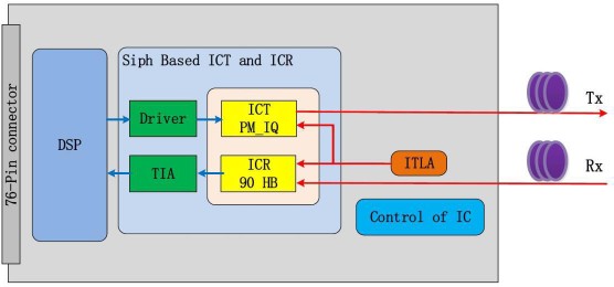
This product uses a 76-pin QSFP-DD MSA QSFP-DD Hardware Specification connector for all electrical interfaces with the host card, whereas the optical interfaces on the line side are provided through the optical receptacles on the QSFP-
DD. The module can be portioned into three functional parts: TX path, RX path and Control& Power block
The host interface is comprised of a total of 8 high-speed SerDes lanes. This allows module to support one interfaces for 400G application: an independent double 4-Lane mode client interfaces (for 400GbE application).
Absolute Maximum Ratings
Parameter | Min. | Max. | Units | Note |
Storage Temperature | -40 | 85 | C | |
Storage Humidity (Relative) | - | 85 | % | no- condensation |
Case Temperature | -5 | 75 | C | |
Operating Humidity (Relative) | - | 85 | % | no- condensation |
Short term Operating Case Temperature | 75 | C | ||
Power Supply Voltage | -0.3 | 3.63 | V | |
RX Optical Maximum Input Power | - | 10 | dBm |
Operating Conditions
Parameter | Min. | Max. | Units | Note |
Operating Case Temperature | 0 | 70 | C | |
Operating Humidity (Relative) | 85 | % | no- condensation | |
Power Supply Operating Range | 3.135 | 3.465 | V | |
RX Optical Input Power | - | 0 | dBm |
Power Supply Specifications
Parameter | Min. | Typ | Max. | Units | Note |
3.3V DC Power Supply Voltage | 3.135 | 3.3 | 3.465 | V | |
3.3V DC Power Supply Current | 7 | A | |||
Power Dissipation | 18.5 | W | |||
Low Power Consumption | 1.0 | W | |||
Module Inrush Current | 100 | mA/us | |||
Turn-off Current | -100 | mA/us | |||
Power Supply Noise | 25 | mV |
Low Speed Control and Sense Signals
Parameter | Symbol | Min | Max | Unit | Condition |
SCL and SDA | VOL | 0 | 0.4 | V | IOL(max)=3 mA for fast mode, 20 mA for Fast-mode plus |
SCL and SDA | VIL | -0.3 | Vcc * 0.3 | V | |
VIH | Vcc * 0.7 | Vcc + 0.5 | V | ||
Capacitance for SCL and SDA I/O signal | Ci | 14 | pF | ||
Total bus capacitive load for SCL and SDA | Cb | 100 | pF | For 300 kHz clock rate use 3.0k Ohms Pill-up resistor, max | |
200 | pF | For 300 kHz clock rate use 3.0k Ohms Pill-up resistor, max | |||
LPMode, ResetL, ModSelL and ePPS | VIL | -0.3 | 0.8 | V | |
VIH | 2 | Vcc + 0.3 | V | ||
LPMode, ResetL and ModSelL | |Iin| | 360 | uA | 0V<Vin<Vcc | |
ePPS | |Iin| | TBD | uA | 0V<Vin<Vcc | |
IntL | VOL | 0 | 0.4 | V | IOL=2.0 mA |
VOH | Vcc – 0.5 | Vcc + 0.3 | V | 10k Ohms pull-up tp Host Vcc | |
ModPrsL | VOL | 0 | 0.4 | V | IOL=2.0 mA |
VOH | V | ModPrsL can be implemented as a short-circuit to GND on the module |
Transceiver Block Diagram
Optical Transmitter Specifications
Parameter | Min. | Typ. | Max. | Units | Note |
Transmitter Frequency Range | 191.3 | 193.7 | 196.1 | THz | C band 75GHz ITU-T grid. Frequencyrange over which the specifications hold unless noted otherwise |
Laser Frequency Stability | -1.8 | 1.8 | GHz | Frequency stability relative to ITU grid | |
Laser Frequency Accuracy | -1.8 | 1.8 | GHz | ||
Laser Frequency Fine TuningRange | -6.0 | 6.0 | GHz | ||
Fine Tuning Resolution | 100 | MHz | |||
Channel Tuning Speed | - | 60 | S | ||
Laser LineWidth | 300 | kHz | |||
Transmitter Output PowerRange | -11.5 | dBm | |||
Transmitter Laser Disable Time | 180 | Ms | |||
Output Power Stability | -0.5 | 0.5 | dB | Difference over temperature, time, wavelength and aging | |
Output Power Accuracy | -2 | 2 | dB | Difference between the set value andactual value over aging | |
Transmitter Turn-up Time from Cold Start | - | 100 | S | ||
Transmitter OSNR (Inband) | 34 | - | dB/0.1m m | ||
Transmitter Back Reflectance | - | -24 | dB | ||
Transmitter Output Power withTX Disabled | - | -20 | dBm | ||
Transmitter Polarization Dependent Power | - | 1.5 | dB | Power deference between X and Ypolarization |
Optical Receiver Specifications
Parameter | Min. | Typ. | Max. | Units | Note |
Receiver Frequency Range | 191.3 | 193.7 | 196.1 | THz | |
Input Power Range | -12 | 0 | dBm | Signal power of the channel at the OSNR Penalty < 0.5dB | |
OSNR Sensitivity | 26 | dB/0.1n m | |||
Receiver Sensitivity | -20 | dBm | Input power needed to achieve postFEC BER < 1E-15 when OSNR Tolerance > 26dB/0.1nm | ||
Los Assert | -20 | -18 | -16 | dBm | |
Los Hysteresis | 1.0 | 2.5 | dB | ||
CD Tolerance | 2400 | ps/nm | Tolerance to Chromatic Dispersion | ||
DGD Tolerance | 10 | ps | Tolerance to PMD with < 0.5 dB penalty to OSNR sensitivity | ||
Peak PDL Tolerance | 3.5 | dB | Tolerance to peak PDL with < 1.3 dBpenalty to OSNR sensitivity when change in SOP is < =1 rad/ms | ||
Tolerance to Change in SOP | 50 | - | rad/ms | ||
Input Power Transient Tolerance | -2 | 2 | dB | Tolerance to change in input powerwith < 0.5 dB penalty to OSNR sensitivity | |
Input Power Reading Accuracy | -2 | 2 | dB | ||
Optical Return Loss | -20 | dB | Optical reflectance at Rx connectorinput | ||
Receiver Turn-up Time from Cold Start | - | 100 | s | From module reset, with valid opticalinput signal present |
Electronical Characteristics for Transmitter
Parameter | Min. | Typ. | Max. | Units | Note |
Signal Rate, each Lane | 26.5625±100ppm | GBaud | |||
Different Peak-Peak Input Voltage Tolerance | 900 | mVpp |
Electronical Characteristics for Receiver
Parameter | Min. | Typ. | Max. | Units | Note |
Signal Rate, each Lane | 26.5625±100ppm | GBaud | |||
Different Peak-Peak Input Voltage Tolerance | 750 | 900 | mVpp | ||
Transition Time, 20% to 80% | 9.5 | ps |
Pin Assignment and Description
The electrical pinout of the QSFP-DD module is shown in Figure 2 below.
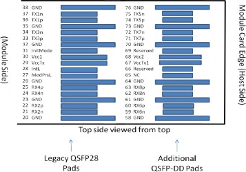
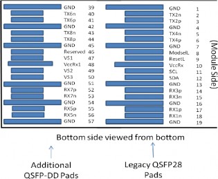
Pin Definition
Pin | Logic | Symbol | Description | Plug Sequence |
1 | GND | Ground | 1B | |
2 | CML-I | Tx2n | Transmitter Inverted Data Input | 3B |
3 | CML-I | Tx2p | Transmitter Non-Inverted Data Input | 3B |
4 | GND | Ground | 1B | |
5 | CML-I | Tx4n | Transmitter Inverted Data Input | 3B |
6 | CML-I | Tx4p | Transmitter Non-Inverted Data Input | 3B |
7 | GND | Ground | 1B | |
8 | LVTTL-I | ModSelL | Module Select | 3B |
9 | LVTTL-I | ResetL | Module Reset | 3B |
10 | VccRx | +3.3V Power Supply Receiver | 2B | |
11 | LVCMOS- I/O | SCL | 2-wire serial interface clock | 3B |
12 | LVCMOS- I/O | SDA | 2-wire serial interface data | 3B |
13 | GND | Ground | 1B | |
14 | CML-O | Rx3p | Receiver Non-Inverted Data Output | 3B |
15 | CML-O | Rx3n | Receiver Inverted Data Output | 3B |
16 | GND | Ground | 1B | |
17 | CML-O | Rx1p | Receiver Non-Inverted Data Output | 3B |
18 | CML-O | Rx1n | Receiver Inverted Data Output | 3B |
19 | GND | Ground | 1B | |
20 | GND | Ground | 1B | |
21 | CML-O | Rx2n | Receiver Inverted Data Output | 3B |
22 | CML-O | Rx2p | Receiver Non-Inverted Data Output | 3B |
23 | GND | Ground | 1B | |
24 | CML-O | Rx4n | Receiver Inverted Data Output | 3B |
25 | CML-O | Rx4p | Receiver Non-Inverted Data Output | 3B |
26 | GND | Ground | 1B | |
27 | LVTTL-O | ModPrsL | Module Present | 3B |
28 | LVTTL-O | IntL | Interrupt | 3B |
29 | VccTx | +3.3V Power supply transmitter | 2B | |
30 | Vcc1 | +3.3V Power supply | 2B | |
31 | LVTTL-I | InitMode | Initialization mode; In legacy QSFP applications, the InitMode pad is called LPMODE | 3B |
32 | GND | Ground | 1B |
33 | CML-I | Tx3p | Transmitter Non-Inverted Data Input | 3B |
34 | CML-I | Tx3n | Transmitter Inverted Data Input | 3B |
35 | GND | Ground | 1B | |
36 | CML-I | Tx1p | Transmitter Non-Inverted Data Input | 3B |
37 | CML-I | Tx1n | Transmitter Inverted Data Input | 3B |
38 | GND | Ground | 1B | |
39 | GND | Ground | 1A | |
40 | CML-I | Tx6n | Transmitter Inverted Data Input | 3A |
41 | CML-I | Tx6p | Transmitter Non-Inverted Data Input | 3A |
42 | GND | Ground | 1A | |
43 | CML-I | Tx8n | Transmitter Inverted Data Input | 3A |
44 | CML-I | Tx8p | Transmitter Non-Inverted Data Input | 3A |
45 | GND | Ground | 1A | |
46 | Reserved | For future use | 3A | |
47 | VS1 | Module Vendor Specific 1 | 3A | |
48 | VccRx1 | 3.3V Power Supply | 2A | |
49 | VS2 | Module Vendor Specific 2 | 3A | |
50 | VS3 | Module Vendor Specific 3 | 3A | |
51 | GND | Ground | 1A | |
52 | CML-O | Rx7p | Receiver Non-Inverted Data Output | 3A |
53 | CML-O | Rx7n | Receiver Inverted Data Output | 3A |
54 | GND | Ground | 1A | |
55 | CML-O | Rx5p | Receiver Non-Inverted Data Output | 3A |
56 | CML-O | Rx5n | Receiver Inverted Data Output | 3A |
57 | GND | Ground | 1A | |
58 | GND | Ground | 1A | |
59 | CML-O | Rx6n | Receiver Inverted Data Output | 3A |
60 | CML-O | Rx6p | Receiver Non-Inverted Data Output | 3A |
61 | GND | Ground | 1A | |
62 | CML-O | Rx8n | Receiver Inverted Data Output | 3A |
63 | CML-O | Rx8p | Receiver Non-Inverted Data Output | 3A |
64 | GND | Ground | 1A | |
65 | NC | No Connect | 3A | |
66 | Reserved | For future use | 3A | |
67 | VccTx1 | 3.3V Power Supply | 2A | |
68 | Vcc2 | 3.3V Power Supply | 2A | |
69 | Reserved | For Future Use | 3A | |
70 | GND | Ground | 1A |
71 | CML-I | Tx7p | Transmitter Non-Inverted Data Input | 3A |
72 | CML-I | Tx7n | Transmitter Inverted Data Input | 3A |
73 | GND | Ground | 1A | |
74 | CML-I | Tx5p | Transmitter Non-Inverted Data Input | 3A |
75 | CML-I | Tx5n | Transmitter Inverted Data Input | 3A |
76 | GND | Ground | 1A |
Digital Diagnostic Functions
The following digital diagnostic characteristics are defined over the normal operating conditions unless otherwise specified.
Parameter | Symbol | Min | Max | Units | Notes |
Temperature monitor absolute error | DMI_Temp | -3 | 3 | degC | Over operating temperature range |
Supply voltage monitor absolute error | DMI _VCC | -0.1 | 0.1 | V | Over full operating range |
Channel RX power monitor absolute error | DMI_RX_Ch | -2 | 2 | dB | 1 |
Channel Bias current monitor | DMI_Ibias_Ch | - 10% | 10% | mA | |
Channel TX power monitor absolute error | DMI_TX_Ch | -2 | 2 | dB | 1 |
Notes:
1. Due to measurement accuracy of different single mode fibers, there could be an additional +/-1 dB fluctuation, or a +/- 3 dB total accuracy.
Mechanical Dimensions

ESD
This transceiver is specified as ESD threshold 1kV for high speed data pins and 2kV for all other electrical input pins, tested per MIL-STD-883, Method 3015.4 /JESD22- A114-A (HBM). However, normal ESD precautions are still required during the handling of this module. This transceiver is shipped in ESD protective packaging. It should be removed from the packaging and handled only in an ESD protected environment.
Laser Safety
This is a Class 1 Laser Product according to EN 60825-1:2014. This product complies with 21 CFR 1040.10 and 1040.11 except for deviations pursuant to Laser Notice No. 50, dated (June 24, 2007).
Caution: Use of controls or adjustments or performance of procedures other than those specified herein may result in hazardous radiation exposure.
Licensing
The following U.S. patents are licensed by Finisar to FluxLight, Inc.:
U.S. Patent Nos: 7,184,668, 7,079,775, 6,957,021, 7,058,310, 6,952,531, 7,162,160, 7,050,720