 Fiber Optic Transceiver")
FINISAR Compatible FTL410QD3C-FL Quick Spec:
FTL410QD3C-FL-EXT FTL410QD3C-FL-IND
Form Factor: QSFP
TX Wavelength: 850nm
Reach: 150m
Cable Type: MMF
Rate Category: 40GBase
Interface Type: SR4
DDM: Yes
Connector Type: MPO
Optical Power Budget: 1.9dB
TX Power Min/Max: -7.6 to +2.4 dBm
RX Power Min/Max: -9.5 to 2.4 dBm
FINISAR Compatible FTL410QD3C-FL Product Features
4 independent full-duplex channels, up to 11.2Gbps data rate per channel
MTP/MPO optical connector
QSFP+ MSA compliant
Digital diagnostic capabilities
Capable of over 100 m transmission on OM3 multi-mode ribbon fiber
CML compatible electrical I/O
Power Dissipation < 1.5W
Single +3.3V power supply
XLPPI electric interface (with 1.5W Max power)
RoHS-6 compliant
Operating case temperature:
Standard 0 to 70oC
Extended -5 to +85 oC
Industrial -40 to +85 oC
FINISAR Compatible FTL410QD3C-FL Applications
Rack to rack, data center
40G Ethernet, Infiniband QDR, DDR and SDR
FINISAR Compatible FTL410QD3C-FL Overview
The FTL410QD3C-FL is a parallel 40Gbps Quad Small Form-factor Pluggable (QSFP+) optical module. It provides increased port density and total system cost savings. The QSFP+ full-duplex optical module offers 4 independent transmit and receive channels, each capable of 10Gbps operation for an aggregate data rate of 40Gbps over 100 meters of OM3 multi-mode fiber. An optical fiber ribbon cable with an MPO/MTPTM connector can be plugged into the QSFP+ module receptacle. Proper alignment is ensured by the guide pins inside the receptacle. Electrical connection is achieved through a z-pluggable 38-pin IPASS® connector. The module operates via a single +3.3V power supply. LVCMOS/LVTTL global control signals, such as Module Present, Reset, Interrupt and Low Power Mode, are available with the modules. A 2-wire serial interface is available to send and receive more complex control signals, and to receive digital diagnostic information. Individual channels can be addressed and unused channels can be shut down for maximum design flexibility. The FTL410QD3C-FL is designed with form factor, optical/electrical connection and digital diagnostic interface according to the QSFP+ Multi-Source Agreement (MSA). It has been designed to meet the harshest external operating conditions including temperature, humidity and EMI interference. The module offers very high functionality and feature
integration, accessible via a two-wire serial interface.
FINISAR Compatible FTL410QD3C-FL Functional Diagram
The FTL410QD3C-FL converts parallel electrical input signals into parallel optical signals, by a driven Vertical Cavity Surface Emitting Laser (VCSEL) array. The transmitter module accepts electrical input signals compatible with Common Mode Logic (CML) levels. All input data signals are differential and internally terminated. The receiver module converts parallel optical input signals via a photo detector array into parallel electrical output signals. The receiver module outputs electrical signals are also voltage compatible with Common Mode Logic (CML) levels. All data signals are differential and support a data rates up to 10 Gbps per channel. Figure 1 shows the functional block diagram of the TR-QQ85S-N00 QSFP+ Transceiver. A single +3.3V power supply is required to power up the module. Both power supply pins VccTx and VccRx are internally connected and should be applied concurrently. As per MSA specifications the module offers 7 low speed hardware control pins (including the 2-wire serial interface): ModSelL, SCL, SDA, ResetL, LPMode, ModPrsL and IntL
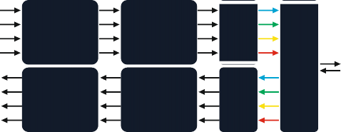
Tx3 Tx2 Tx1 Tx0
Rx3 Rx2 Rx1 Rx0
MM ribbon Fiber cable
Module Select (ModSelL) is an input pin. When held low by the host, the module responds to 2-wire serial communication commands. The ModSelL allows the use of multiple QSFP+ modules on a single 2-wire interface bus – individual ModSelL lines for each QSFP+ module must be used. Serial Clock (SCL) and Serial Data (SDA) are required for the 2-wire serial bus communication interface and enable the host to access the QSFP+ memory map. The ResetL pin enables a complete module reset, returning module settings to their default state, when a low level on the ResetL pin is held for longer than the minimum pulse length. During the execution of a reset the host shall disregard all status bits until the module indicates a completion of the reset interrupt. The module indicates this by posting an IntL (Interrupt) signal with the Data_Not_Ready bit negated in the memory map. Note that on power up (including hot insertion) the module should post this completion of reset interrupt without requiring a reset. Low Power Mode (LPMode) pin is used to set the maximum power consumption for the module in order to protect hosts that are not capable of cooling higher power modules, should such modules be accidentally inserted. Module Present (ModPrsL) is a signal local to the host board which, in the absence of a module, is normally pulled up to the host Vcc. When a module is inserted into the connector, it completes the path to ground though a resistor on the host board and asserts the signal. ModPrsL then indicates a module is present by setting ModPrsL to a “Low” state. Interrupt (IntL) is an output pin. Low indicates a possible module operational fault or a status critical to the host system. The host identifies the source of the interrupt using the 2-wire serial interface. The IntL pin is an open collector output and must be pulled to the Host Vcc voltage on the Host board.
Absolute Maximum Ratings
Parameter | Symbol | Min | Max | Unit |
Storage Temperature | Ts | -40 | +85 | oC |
Power Supply Voltage | Vcc | -0.5 | 3.6 | V |
Input Voltage) | VIN | -0.5 | Vcc | V |
Damage Threshold, each Lane | THd | 2.4 | dBm |
Recommended Operating Conditions
Parameter | Symbol | Min | Typ | Max | Unit |
Operating Case Temp (Standard) | TOP | 0 | 70 | oC | |
Operating Case Temp (Industrial) | TOP | -40 | 85 | oC | |
Power Supply Voltage | Vcc | 3.1 | 3.3 | 3.5 | V |
Baud Rate | 10.3125 | 11.2 | Gb/s | ||
Link Distance with OM3 MMF | D | 100 | m | ||
Link distance with OM4 MMF | D | 150 | m |
Recommended Power Supply Filter
 Fiber Optic Transceiver")
Electrical Characteristics
Parameter | Symbol | Min | Typ | Max | Unit |
Power Consumption | 0 | 1.5 | W | ||
Supply Current | Icc | 350 | mA |
Electrical Characteristics – Transmitter (each lane)
Parameter | Symbol | Min Typ Max | Unit | Notes | ||
Single-ended Input Voltage Tolerance (Note 2) | -0.3 | 4.0 | V | Referred to TP1 signal common | ||
AC Common Mode Input Voltage Tolerance (RMS) | 15 | mV | RMS | |||
Differential Input Voltage Swing Threshold | 50 | mVpp | LOSA Threshold | |||
Differential Input Voltage Swing | Vin,pp | 190 | 700 | mVpp | ||
Differential Input Impedance | Zin | 90 | 100 | 110 | Ω | |
Differential Input Return Loss | See IEEE 802.3ba 86A.4.1.1 | dB | 10MHz - 11.1GHz | |||
J2 Jitter Tolerance | Jt2 | 0.17 | UI | |||
J9 Jitter Tolerance | Jt9 | 0.29 | UI | |||
Data Dependent Pulse Width Shrinkage (DDPWS) Tolerance | 0.07 | UI | ||||
Eye Mask Coordinates {X1, X2, Y1, Y2} | 0.11, 0.31 95, 350 | UI mV | ||||
Electrical Characteristics – Receiver (each lane)
Parameter | Symbol | Min | Typ | Max | Unit | Notes |
Single-ended Output Voltage Threshold | -0.3 | 4.0 | V | Referred to signal common | ||
AC Common Mode Output Voltage Tolerance (RMS) | 7.5 | mV | RMS | |||
Differential Output Voltage Swing Threshold | Vout,pp | 300 | 850 | mVpp | ||
Differential Output Impedance | Aout | 90 | 100 | 110 | Ohm | |
Termination Mismatch at 1MHz | 5 | % | ||||
Differential Output Return Loss | See IEEE 802.3ba 86A.4.2.1 | 10MHz - 11.1GHz | ||||
Common mode Output Return Loss | See IEEE 802.3ba 86A.4.2.2 | 10MHz - 11.1GHz | ||||
Output Transition Time | 28 | ps | 20% to 80% | |||
J2 Jitter Tolerance | Jo2 | 0.42 | UI | |||
J9 Jitter Tolerance | Jo9 | 0.65 | UI | |||
Eye Mask Coordinates {X1, X2, Y1, Y2} | 0.29, 05 150, 425 | UI mV | Hit Ratio = 5x10⁻⁵ | |||
Notes:
Power-on initialization time is the time from when the power supply voltages reach and remain above the minimum recommended operating supply voltages to the time when the moduleis fully functional.
The single ended input voltage tolerance is the allowable range of the instantaneous input signals.
FINISAR Compatible FTL410QD3C-FL Optical Characteristics – Transmitter
Parameter | Symbol | Min | Typ | Max | Unit | Notes |
Center Wavelength | λ0 | 840 | 850 | 860 | nm | |
RMS Spectral Width | Rm | 0.5 | 0.65 | nm | ||
Average Launch Power (each Lane) | PAVG | -7.6 | -2 | +1 | dBm | |
Optical Modulation Amplitude (OMA) (each Lane) | POMA | -5.6 | +3 | dBm | ||
Peak Power (each Lane) | PPt | +4 | dBm | |||
Launch Power in OMA minus Transmitter and Dispersion Penalty (TDP), each Lane | -6.5 | dB | ||||
TDP (each Lane) | 3.5 | dB | ||||
Extinction Ratio | ER | 3 | dB | |||
Relative Intensity Noise | RIN | -128 | dB/Hz | 12dB reflection | ||
Optical Return Loss Tolerance | 12 | dB | ||||
Transmitter Eye Mask Definition {X1, X2, X3, Y1, Y2, Y3} | {0.23, 0.34, 0.43, 0.27, 0.35, 0.4} | |||||
Average Launch Power OFF (each Lane) | Poff | -30 | dBm | |||
Note: Transmitter optical characteristics are measured with a single mode fiber.
FINISAR Compatible FTL410QD3C-FL Optical Characteristics - Receiver
Parameter | Symbol | Min | Typ | Max | Unit | Notes |
Center Wavelength | λ0 | 840 | 850 | 860 | dBm | |
Damage Threshold | Thd | 3.4 | dBm | |||
Average Receive Power (each Lane) | -9.5 | +2.4 | dBm | |||
Receiver Reflectance | RR | -12 | dB | |||
Receive Power (OMA) (each Lane) | 3 | dBm | ||||
Receiver Sensitivity in OMA (each Lane) | SEN | -5.4 | dBm | |||
Receiver Sensitivity per Channel | PSens | -12 | -10 | dB | ||
LOS Assert | LOSA | -21 | -16 | dBm | ||
LOS Deassert | LOSD | -19 | -13 | dBm | ||
LOS Hysteresis | LOSH | 0.5 | dB | |||
Receiver Electrical 3dB upper cut-off Frequency (each Lane) | Fc | 12.3 | GHz |
Notes:
Even if the TDP < 0.8 dB, the OMA min must exceed theminimum value specified here.
The receiver shall be able to tolerate, without damage, continuous exposure to a modulated optical input signal having this power level on one lane. The receiver does not have to operate correctly at this input power.
Measured with conformance test signal at receiver inputfor BER = 1x10-12.
Vertical eye closure penalty and stressed eye jitter are test conditions for measuring stressed receiver sensitivity. They are not characteristics of the receiver.
FINISAR Compatible FTL410QD3C-FL Digitial Diagnostics Function
The following digital diagnostic characteristics are defined over the normal operating conditions unless otherwise
specified.
Parameter | Symbol | Min | Typ | Max | Unit | Notes |
Temperature monitor absolute error | DMITEMP | -3 | 3 | deg. C | Over operating temperature range | |
Supply voltage monitor absolute error | DMIVCC | -0.1 | 0.1 | V | Over Full operating range | |
Channel RX power monitor absolute error | DMIRX_CH | -2 | 2 | dB | 1 | |
Channel Bias current monitor | DMIIbias_CH | -10% | 10% | mA | ||
Channel TX power monitor absolute error | DMITX_CH | -2 | 2 | dB | 1 |
Note 1: Due to measurement accuracy of different multi-mode fibers, there could be an additional ±1dB fluctuation, or ± 3dB total accuracy.
Mode-Conditioning Patch Cable
Figure 2. shows the orientation of the multi-mode facets of the optical connector
 Fiber Optic Transceiver")
Figure 2 Optical connector
Fiber | Description | PIN | Description |
1 | Rx (0) | 7 | Not used |
2 | Rx (1) | 8 | Not used |
3 | Rx (2) | 9 | Tx (3) |
4 | Rx (3) | 10 | Tx (2) |
5 | Not used | 11 | Tx (1) |
6 | Not used | 12 | Tx (0) |
FINISAR Compatible FTL410QD3C-FL Optical and Electrical Characteristics
Parameter | Symbol | Min | Typ | Max | Unit |
50 / 125 um MMF | 300 | m | |||
Data Rate | 10.3125 | Gbps |
![]()
FINISAR Compatible FTL410QD3C-FL Optical and Electrical Characteristics - Transmitter
Parameter | Symbol | Min | Typ | Max | Unit |
Centre Wavelength | C | 840 | 850 | 860 | nm |
Spectral Width (RMS) |
| 0.45 | nm | ||
Average Output Power | Pout | -6 | -1 | dBm | |
Extinction Ratio | Er | 3.0 | 5.0 | dB | |
Output Optical Eye IEEE 802.3-2005 Compliant | |||||
Transmitter Dispersion Penalty | TDP | 3.9 | dB | ||
Input Differential Impedance | ZIN | 90 | 100 | 110 | Ω |
TX_Disable Assert Time | t_off | 10 | us | ||
TX_DISABLE Negate Time | t_on | - | - | 1 | ms |
TX_BISABLE time to start reset | t_reset | 10 | - | - | us |
Time to initialize, include reset of TX_FAULT | t_init | - | - | 300 | ms |
TX_FAULT from fault to assertion | t_fault | - | - | 100 | us |
Total Jitter | TJ | - | - | 0.28 | UI(p-p) |
Data Dependant Jitter | DDJ | - | - | 0.1 | UI(p-p) |
Uncorrelated Jitter | UJ | - | - | 0.023 | RMS |
![]()
FINISAR Compatible FTL410QD3C-FL Optical and Electrical Characteristics - Receiver
Parameter | Symbol | Min | Typ | Max | Unit |
Centre Wavelength | C | 840 | 850 | 860 | nm |
Receiver Sensitivity | Pmin | -11.1 | dBm | ||
Output Differential Impedance | RIN | 90 | 100 | 110 | Ω |
Receiver Overload2 | Pmax | -1 | dBm | ||
Optical Return Loss | ORL | -12 | dB | ||
LOS De-Assert | LOSD | -12.5 | dBm | ||
LOS Assert | LOSA | 25 | dBm | ||
LOS Hysteresis | 0.5 | dB | |||
LOS | High | 2.0 | VCC+0.3 | V | |
Low | 0 | 0.8 |
PIN Assignment and Function Definitions
PIN Assignment
 Fiber Optic Transceiver")
PIN Definition
PIN | Signal Name | Description |
1 | GND | Ground (1) |
2 | Tx2n | CML-I Transmitter 2 Inverted Data Input |
3 | Tx2p | CML-I Transmitter 2 Non-Inverted Data Input |
4 | GND | Ground (1) |
5 | Tx4n | CML-I Transmitter 4 Inverted Data Input |
6 | Tx4p | CML-I Transmitter 4 Non-Inverted Data Input |
7 | GND | Ground (1) |
8 | ModSelL | LVTLL-I Module Select |
9 | ResetL | LVTLL-I Module Reset |
10 | VCCRx | +3.3V Power Supply Receiver (2) |
11 | SCL | LVCMOS-I/O 2-Wire Serial Interface Clock |
12 | SDA | LVCMOS-I/O 2-Wire Serial Interface Data |
13 | GND | Ground (1) |
14 | Rx3p | CML-O Receiver 3 Non-Inverted Data Output |
15 | Rx3n | CML-O Receiver 3 Inverted Data Output |
16 | GND | Ground (1) |
17 | Rx1p | CML-O Receiver 1 Non-Inverted Data Output |
18 | Rx1n | CML-O Receiver 1 Inverted Data Output |
19 | GND | Ground (1) |
20 | GND | Ground (1) |
21 | Rx2n | CML-O Receiver 2 Inverted Data Output |
22 | Rx2p | CML-O Receiver 2 Non-Inverted Data Output |
23 | GND | Ground (1) |
24 | Rx4n | CML-O Receiver 4 Inverted Data Output |
25 | Rx4p | CML-O Receiver 4 Non-Inverted Data Output |
26 | GND | Ground (1) |
27 | ModPrsL | Module Present |
28 | IntL | Interrupt |
29 | VCCTx | +3.3V Power Supply Transmitter (2) |
30 | VCC1 | +3.3V Power Supply |
31 | LPMode | LVTLL-I Low Power Mode |
32 | GND | Ground (1) |
33 | Tx3p | CML-I Transmitter 3 Non-Inverted Data Input |
34 | Tx3n | CML-I Transmitter 3 Inverted Data Input |
35 | GND | Ground (1) |
36 | Tx1p | CML-I Transmitter 1 Non-Inverted Data Input |
37 | Tx1n | CML-I Transmitter 1 Inverted Data Input |
38 | GND | Ground (1) |
Notes:
All Ground (GND) are common within the QSFP+ module and all module voltages are referenced to this potential unless noted otherwise. Connect these directly to the host board signal common ground plane.
VccRx, Vcc1 and VccTx are the receiving and transmission power suppliers and shall be applied concurrently. The connector pins are each rated for a maximum current of 500mA.
Licensing
The following U.S. patents are licensed by Finisar to FluxLight, Inc.:
U.S. Patent Nos: 7,184,668, 7,079,775, 6,957,021, 7,058,310, 6,952,531, 7,162,160, 7,050,720