
Cisco Compatible SFP-25GBX-U-10 Quick Spec:
Part Number: SFP28-25GBASE-BX-10 SFP28-25GBASE-BX-10-EXT SFP28-25GBASE-BX-10-IND
Form Factor: SFP28
TX Wavelength: 1270/1330nm
Reach: 10km
Cable Type: SMF
Rate Category: 25GBase
Interface Type: BX
DDM: Yes
Connector Type: Single-LC
Cisco Compatible SFP-25GBX-U-10 Features
Supports 25.78125Gb/s serial optical interface
Up to 10km transmission on SMF
Un-cooled DFB laser and PIN receiver
Hot-pluggable SFP28 footprint
Built-in digital diagnostic functions
Single +3.3V power supply
Power consumption less than 1.2 W
Operating case temperature
Standard: 0°C to +70 °C
Extended -5°C to +85 °C
Industrial -40°C to +85 °C
Internal CDR on both transmitter and receiver channel
Support CDR bypass
SFP28 MSA package with simplex LC connector, Bi-directional
Compliant with SFF-8402 and SFF-8472
Compliant to SFF-8431 and SFF-8432
Compliant with IEEE 802.3by 25GBASE-LR
Compliant with FCC 47 CFR Part 15, Class B
Compliant with Telcordia GR-468-CORE
RoHS Compliant
Cisco Compatible SFP-25GBX-U-10 Applications
25GBASE-BX 25G Ethernet
25.78125 Gb/s single lane 100GE LR4
Other optical links
The SFP28 transceivers are high performance, cost effective modules supporting data rate of 25.78125Gbps and 10km transmission distance with SMF. The transceiver consists of three sections: a Un-cooled DFB laser transmitter, a PIN photodiode integrated with a trans-impedance preamplifier (TIA) and MCU control unit. All modules satisfy y class I laser safety requirements. The transceivers are compatible with SFP Multi-Source Agreement and SFF-8472 digital diagnostics functions.
.png")
Figure 1. Transceiver functional Block Diagram
(Exceeding the limits below may damage the transceiver module permanently)
Parameter | Symbol | Min | Typ | Max | Unit | Notes |
Maximum Supply Voltage | VCC | -0.5 | - | +4.0 | V | |
Storage Temperature | TS | -40 | - | +85 | °C | |
Case Operating Temperature- Commercial | TA | 0 | - | +70 | °C | |
Case Operating Temperature-Industrial | TA | -40 | - | +85 | °C | |
Relative Humidity | RH | 5 | - | 85 | % | 1 |
Notes:
Non-condensing.
Recommend Operation Environment
Parameter | Symbol | Min | Typ | Max | Unit | Notes |
Data Rate | BR | - | 25.78125 | - | Gbps | |
Power Supply Voltage | VCC | 3.13 | 3.3 | 3.47 | V | |
Power Supply Current | ICC | - | - | 350 | mA | |
Power Dissipation | PD | - | - | 1.2 | W | |
Case Operating Temperature | TA | -5 | - | +70 | °C | |
Transmission Distance | TD | - | - | 10 | km | 1 |
Notes:
Measured with ITU-T G.652 SMF
Electricalptical Characteristics
Parameter | Symbol | Min | Typ | Max | Unit | Notes |
Transmitter | ||||||
Differential Data Input Amplitude | VIN,P-P | 180 | - | 1200 | mVpp | 1 |
Input Differential Impedance | ZIN | 90 | 100 | 110 | Ω | |
Transmitter Fault Output-High | VOH | 2.0 | - | VCC | V | |
Transmitter Fault Output-Low | VOL | 0 | - | 0.8 | V | |
Transmitter Disable Voltage- High | VIH | 2.0 | - | VCC | V | |
Transmitter Disable Voltage- low | VIL | 0 | - | 0.8 | V | |
Receiver | ||||||
Differential output voltage swing | VOUT,P-P | 300 | - | 850 | mVpp | 1 |
Output Differential Impedance | ZOUT | 90 | 100 | 110 | Ω | |
Deterministic Jitter | DJ | - | - | 0.42 | UI | |
Total Jitte | TJ | - | - | 0.70 | UI | |
LOS Output Voltage-High | VLOSH | 2.0 | - | VCC | V | |
LOS Output Voltage-Low | VLOSL | - | - | 0.8 | V | |
Notes:
CML input/output, internally AC-coupled and terminated.
Parameter | Symbol | Min | Typ | Max | Unit | Notes |
Transmitter | ||||||
Optical Center Wavelength (LR2733) | λC | 1260 | 1270 | 1280 | nm | |
Optical Center Wavelength (LR3327) | λC | 1320 | 1330 | 1340 | nm | |
Data Rate | BR | - | 25.78125 | - | Gbps | |
Average Output Power | PO | -7.0 | - | +2.0 | dBm | |
Optical Modulation Amplitude | POMA | -4.0 | - | +2.2 | dBm | |
Optical Extinction Ratio | ER | 3.5 | - | - | dB | |
RMS Spectral Width (-20dB) | Δσ | - | - | 1.0 | nm | |
Side Mode Suppression Ratio | SMSR | 30 | - | - | dB | |
Relative Intensity Noise | RIN | - | - | -130 | dB/Hz | |
Optical Return Loss Tolerance | ORL | - | - | 20 | dB | |
Transmitter Reflectance | RT | - | - | -12 | dB | |
Average Launch power of Tx OFF | POFF | - | - | -30 | dBm | |
Optical Eye Mask | Compliant with IEEE 802.3by | |||||
Receiver | ||||||
Center Wavelength Range (LR2733) | λC | 1320 | - | 1340 | nm | |
Center Wavelength Range (LR3327) | λC | 1260 | - | 1280 | nm | |
Data Rate | BR | - | 25.78125 | - | Gbps | |
Maximum Receiver Power (OMA) | RPOMA | - | - | +2.2 | dBm | 1 |
Average Receive Power | RPO | -11.3 | - | +2.0 | dBm | |
Receiver Sensitivity (OMA) | RSENS | - | - | -11.3 | dBm | |
Stressed Receiver Sensitivity (OMA) | RSRS | - | - | -8.8 | dBm | 1 |
LOS Assert | LOSA | -25 | - | - | dBm | |
LOS De-Assert | LOSD | - | - | -15 | dBm | |
LOS Hysteresis | LOSH | 0.5 | - | 5 | dB | |
Receiver Reflectance | RR | - | - | -26 | dB | |
Notes:
For 25G-LR with FEC, receiver sensitivity is defined at 5E-5 BER level, not 10-12 BER level.
Parameter | Symbol | Min | Typ | Max | Unit |
Tx Disable Negate Time | t_on | - | - | 1 | ms |
Tx Disable Assert Time | t_off | - | - | 10 | µs |
Time To Initialize, including Reset of Tx Fault | t_init | - | - | 300 | ms |
Tx Fault Assert Time | t_fault | - | - | 100 | µs |
Tx Fault To Reset | t_reset | 10 | - | - | µs |
LOS Assert Time | t_loss_on | - | - | 100 | µs |
LOS De-assert Time | t_loss_off | - | - | 100 | µs |
Rate-Select Change Time | t_ratesel | - | - | 10 | µs |
Serial ID Clock Rate | f_serial_clock | - | 100 | 400 | KHZ |
SDA, SCL, MOD_ABS High Level | VH | 2.0 | - | VCC | V |
SDA, SCL, MOD_ABS Low Level | VL | - | - | 0.8 | V |
1. Open collector/drain output, which should be pulled up with a 4.7kΩ to 10kΩ resistor on the host board if intended for use. Pull up voltage should be between 2.0V to 3.6V. A high output indicates a transmitter fault caused by either the TX bias current or the TX output power exceeding the preset alarm thresholds. A low output indicates normal operation. In the low state, the output is pulled to <0.8V.
Laser output disabled on Tx_Disable >2.0V or open, enabled on Tx_Disable <0.8V.
LOS is open collector output. Should be pulled up with 4.7kΩ to 10kΩ on host board to a voltage between 2.0V and 3.6V. Logic 0 indicates normal operation; logic 1 indicates loss of signal.
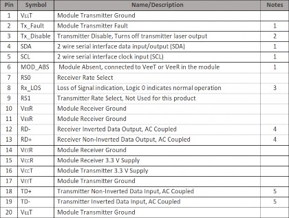
RD-/+: These are the differential receiver outputs. They are internally AC-coupled 100Ω differential lines which should be terminated with 100Ω (differential) at the user SERDES.
TD-/+: These are the differential transmitter inputs. They are internally AC-coupled, differential lines with 100Ω differential termination inside the module.


Figure 2. Host PCB SFP+ pad assignment top view and Names.
The transceivers provide serial ID memory contents and diagnostic information about the present operating conditions by the 2-wire serial interface (SCL, SDA).
The diagnostic information with internal calibration or external calibration all are implemented, including received power monitoring, transmitted power monitoring, bias current monitoring, supply voltage monitoring and temperature monitoring. The digital diagnostic memory map specific data field defines as following.

Parameter | Calibration | Range | Accuracy | Unit |
Transceiver Internal Temperature | Internal | -5 to +70°C | ±3.0 | °C |
VCC3 Internal Supply Voltage | Internal | 3.0 to 3.6V | ±3.0 | % |
Laser Bias Current | Internal | 0 to 90mA | ±10 | % |
Tx Output Power | Internal | -7.0 to +3.0dBm | ±3.0 | dBm |
Rx Input Power | Internal | -14.0 to +3.0dBm | ±3.0 | dBm |
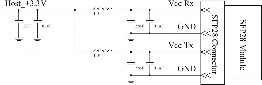
Figure 3, Recommended Host Board Power Supply Circuit
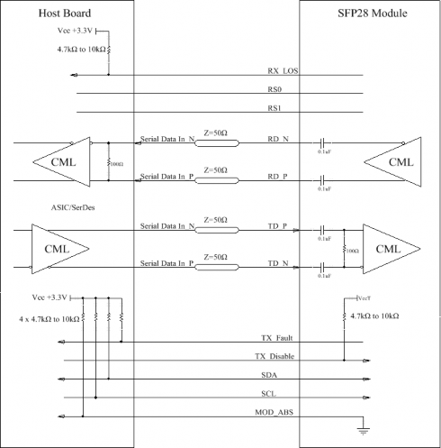
Figure 4, Recommended Interface Circuit

Figure 5, Mechanical Dimensions
Handling Precautions: This device is susceptible to damage as a result of electrostatic discharge (ESD). A static free environment is highly recommended. Follow guidelines according to proper ESD procedures.
Laser Safety: Radiation emitted by laser devices can be dangerous to human eyes. Avoid eye exposure to direct or indirect radiation.
The following U.S. patents are licensed by Finisar to FluxLight, Inc.:
U.S. Patent Nos: 7,184,668, 7,079,775, 6,957,021, 7,058,310, 6,952,531, 7,162,160, 7,050,720