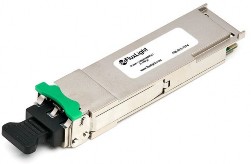
Part #: QSFP-100G-CWDM4-S QSFP-100G-CWDM4-S-EXT QSFP-100G-CWDM4-S-IND
Form Factor: QSFP28
TX Wavelength: CWDM4
Reach: 2km
Cable Type: SMF
Rate Category: 100GBase
Interface Type: CWDM4
DDM: Yes
Connector Type: Dual-LC Optical Power Budget: 7.5 dB
TX Power Min/Max: -4.00 to +2.50 dBm RX Power Min/Max: -11.50 to +3.50 dBm
Cisco Compatible QSFP-100G-CWDM4-S Features:
Hot pluggable QSFP28 MSA form factor
Supports 103 Gbps
Up to 2km reach for G.652 SMF
Single +3.3V power supply
Transmitter: cooled 4x25 Gbps CWDM DML TOSA (1270, 1290, 1310, 1330nm)
Receiver: 4x25 Gbps PIN ROSA
4x25G Electrical Serial Interface
Maximum power consumption 3.5W
RoHS-6 compliant (lead-free)
Duplex LC receptacle
I2C interface with integrated Digital Diagnostic Monitoring
Operating Case Temperature
Standard 0 to +70 °C
Extended -4 to +85 °C
Industrial -40 to +85 °C
Cisco Compatible QSFP-100G-CWDM4-S Applications:
100GBASE-LR4 Ethernet links
Cisco Compatible QSFP-100G-CWDM4-S Overview
The QSFP-100G-CWDM4-S is a 103 Gbps transceiver module designed for optical communication applications compliant to 100GBASE-CWDM4 of the IEEE P802.3ba standard. The module converts 4 input channels of 25 Gbps electrical data to 4 optical CWDM channels and then multiplexes them into a single channel for 103 Gbps optical transmission. Reversely on the receiver side, the module de-multiplexes a 103 Gbps optical input into 4 channels of CWDM optical signals and then converts them to 4 output channels of electrical data. The central wavelengths of the 4 LAN WDM channels are 1270, 1290, 1310 and 1330 nm as members of the CWDM wavelength grid. The high performance cooled DML DFB
transmitters and high sensitivity PIN receivers provide superior performance for 100G applications up to 2km links. The product is designed with form factor, optical/electrical connection and digital diagnostic interface per the QSFP+ Multi- Source Agreement (MSA).
Cisco Compatible QSFP-100G-CWDM4-S Specification: Absolute Maximum Ratings
Parameter | Symbol | Min | Max | Unit |
Storage Temperature | Ts | -40 | +85 | °C |
Operating Case Temp (Standard) | TOP | 0 | 70 | °C |
Operating Case Temp (Industrial) | TOP | -40 | 85 | °C |
Power Supply Voltage | Vcc | -0.5 | 3.6 | V |
Relative Humidity (non- condensation) | RH | 5 | 85 | % |
Recommended Operating Conditions
Parameter | Symbol | Min | Typ | Max | Unit |
Power Supply Voltage | Vcc | 3.135 | 3.3 | 3.465 | V |
Data Rate, each Lane | 25.78125 | Gb/s | |||
Control Input Voltage High) | 2 | Vcc | V | ||
Control Input Voltage Low | 0 | 0.8 | V | ||
Link Distance with (SM fiber) | D | 2 | km |
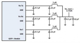
Recommended Power Supply Filter
Electrical Characteristics
Parameter | Symbol | Min | Typ | Max | Unit |
Power Consumption | - | 4.5 | W | ||
Supply Current | Icc | 1.21 | A |
Electrical Characteristics – Transmitter (each lane)
Parameter | Symbol | Min | Typ | Max | Unit |
Differential Input Voltage Swing | Vin.pp | 150 | 1200 | mVpp | |
Differential Input Impedance | Zin | 85 | 100 | 115 | Ω |
Electrical Characteristics-Receiver
Parameter | Symbol | Min | Typ | Max | Unit |
Differential Output Voltage Swing | Vout.pp | 200 | 1100 | mVpp | |
Differential Output Impedance | Zout | 85 | 100 | 115 | ohm |
Optical Characteristics
Parameter | Symbol | Min | Typ | Max | Unit |
Lane Wavelength | L0 | 1264.5 | 1270 | 1277.5 | nm |
L1 | 1284.5 | 1290 | 1297.5 | ||
L2 | 1304.5 | 1310 | 1317.5 | ||
L3 | 1324.5 | 1330 | 1337.5 |
Optical Characteristics-Transmitter
Parameter | Symbol | Min | Typ | Max | Unit | Notes |
Signaling Speed per Lane | BR | 25.78 | Gbps | |||
Side-mode Suppression Ratio | SMSR | 30 | dB | |||
Total Average Launch Power | PT | 8.5 | dBm | |||
Average Launch Power (each Lane) | PAVG | -6.5 | 2.5 | dBm | ||
Optical Modulation Amplitude (each Lane) | POMA | -4.0 | 2.5 | dBm | 1 | |
Extinction Ratio | ER | 3.5 | dB | |||
Optical Return Loss Tolerance | TOL | 20 | dB | |||
Eye Mask {X1, X2, X3, Y1, Y2, Y3} | IEEE 802.3 Clause 88 100GBase-LR4 | |||||
Average Launch Power OFF (each Lane) | Poff | -30 | dBm | |||
Optical Characteristics-Receiver
Parameter | Symbol | Min | Typ | Max | Unit | Notes |
Signaling Speed per Lane | BR | 25.78 | Gbps | |||
Damage threshold per lane | 5.5 | dBm | ||||
Average Power at Receiver, each Lane | -11.5 | 2.5 | dBm | |||
Receive Power (OMA) (each Lane) | 4.5 | dBm | ||||
Receiver Sensitivity (OMA), each Lane | SEN | -10 | dBm | |||
LOS Assert | LOSA | -20.6 | dBm | |||
LOS Deassert | LOSD | -11.6 | dBm | |||
LOS Hysteresis | LOSH | 0.5 | dB | |||
Optical Return Loss | ORL | -25 | dB |
Digital Diagnostic Functions
The following digital diagnostic characteristics are defined over the normal operating conditions unless otherwise specified.
Parameter | Symbol | Min | Typ | Max | Unit | Notes |
Temperature monitor absolute error | DMITEMP | -3 | 3 | deg. C | Over operating temperature range | |
Supply voltage monitor absolute error | DMIVCC | -0.1 | 0.1 | V | Over Full operating range | |
Channel RX power monitor absolute error | DMIRX_CH | -2 | 2 | dB | 1 | |
Channel Bias current monitor | DMIIbias_CH | -10% | 10% | mA | ||
Channel TX power monitor absolute error | DMITX_CH | -2 | 2 | dB | 1 |
PIN Assignment and Function Definitions
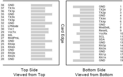
PIN Definition
PIN | Signal Name | Description |
1 | GND | Ground (1) |
2 | Tx2n | CML-I Transmitter 2 Inverted Data Input |
3 | Tx2p | CML-I Transmitter 2 Non-Inverted Data Input |
4 | GND | Ground (1) |
5 | Tx4n | CML-I Transmitter 4 Inverted Data Input |
6 | Tx4p | CML-I Transmitter 4 Non-Inverted Data Input |
7 | GND | Ground (1) |
8 | ModSelL | LVTLL-I Module Select |
9 | ResetL | LVTLL-I Module Reset |
10 | VCCRx | +3.3V Power Supply Receiver (2) |
11 | SCL | LVCMOS-I/O 2-Wire Serial Interface Clock |
12 | SDA | LVCMOS-I/O 2-Wire Serial Interface Data |
13 | GND | Ground (1) |
14 | Rx3p | CML-O Receiver 3 Non-Inverted Data Output |
15 | Rx3n | CML-O Receiver 3 Inverted Data Output |
16 | GND | Ground (1) |
17 | Rx1p | CML-O Receiver 1 Non-Inverted Data Output |
18 | Rx1n | CML-O Receiver 1 Inverted Data Output |
19 | GND | Ground (1) |
20 | GND | Ground (1) |
21 | Rx2n | CML-O Receiver 2 Inverted Data Output |
22 | Rx2p | CML-O Receiver 2 Non-Inverted Data Output |
23 | GND | Ground (1) |
24 | Rx4n | CML-O Receiver 4 Inverted Data Output |
25 | Rx4p | CML-O Receiver 4 Non-Inverted Data Output |
26 | GND | Ground (1) |
27 | ModPrsL | Module Present |
28 | IntL | Interrupt |
29 | VCCTx | +3.3V Power Supply Transmitter (2) |
30 | VCC1 | +3.3V Power Supply |
31 | LPMode | LVTLL-I Low Power Mode |
32 | GND | Ground (1) |
33 | Tx3p | CML-I Transmitter 3 Non-Inverted Data Input |
34 | Tx3n | CML-I Transmitter 3 Inverted Data Input |
35 | GND | Ground (1) |
36 | Tx1p | CML-I Transmitter 1 Non-Inverted Data Input |
37 | Tx1n | CML-I Transmitter 1 Inverted Data Input |
38 | GND | Ground (1) |
Notes:
All Ground (GND) are common within the QSFP+ module and all module voltages are referenced to this potential
unless noted otherwise. Connect these directly to the host board signal common ground plane.
VccRx, Vcc1 and VccTx are the receiving and transmission power suppliers and shall be applied concurrently. The connector pins are each rated for a maximum current of 500mA.
Licensing
The following U.S. patents are licensed by Finisar to FluxLight, Inc.:
U.S. Patent Nos: 7,184,668, 7,079,775, 6,957,021, 7,058,310, 6,952,531, 7,162,160, 7,050,720