 Fiber Optic Transceiver")
Cisco Compatible QDD-400G-SR4.2-BD-FL Quick Spec:
Part Number: QDD-400G-SR4.2-BD-FL QDD-400G-SR4.2-BD-EXT-FL QDD-400G-SR4.2-BD-IND-FL
Form Factor: QSFP56-DD
TX Wavelength: BiDi 850nm/908nm
Reach: 150m
Cable Type: MMF
Rate Category: 400GBase
Interface Type: SR4.2
DDM: Yes
Connector Type: MPO-12
Cisco Compatible QDD-400G-SR4.2-BD-FL Features
QSFP56-DD MSA compliant
8 Bi-Directional Optical Lanes
IEEE802.3bs Specification compliant
Up to 150m transmission on OM5 Multimode Fiber
8x53.125Gb/s electrical interface (400GAUI-8)
Maximum power consumption 12W
MPO-12 connector
RoHS compliant
Operating Case Temperature
Standard: 0°C to +70 °C
Extended -5°C to +85 °C
Industrial -40°C to +85 °C
Cisco Compatible QDD-400G-SR4.2-BD-FL Applications
400G Ethernet
Infiniband interconnects
Datacenter Enterprise networking
Cisco Compatible QDD-400G-SR4.2-BD-FL General Description
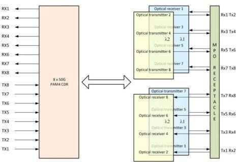
This product can support 400Gb/s bit rates. It is a parallel Quad Small Form-factor Pluggable—double density (QSFP-DD) Bi-Directional optical module. The module accepts eight host electrical data and transmits them in two groups of optical bi-directional lanes (each group contains 4 pairs of optical lane) to allow optical communication over optical multi-mode fibers. Reversely, on the receiver side, the module accepts 8 sets of optical input signal and converts them to 8 channels of electrical data.
An optical fiber with an MPO-12 connector can be plugged into the QSFP-DD module receptacle. Proper alignment is ensured by the guide pins inside the receptacle. The cable usually cannot be twisted for proper channel to channel alignment. Electrical connection is achieved through an MSA-compliant 76-pin edge type connector.
The module operates by a single +3.3 V power supply. LVCMOS/LVTTL global control signals, such as Module Present, Reset, Interrupt and Low Power Mode, are available with the modules. A 2-wire serial interface is available to send and receive more complex control signals, and to receive digital diagnostic information. Individual channels can be addressed and unused channels can be shut down for maximum design flexibility.
The product is designed with form factor, optical/electrical connection and digital diagnostic interface according to
the QSFP56 Multi-Source Agreement (MSA). It has been designed to meet the harshest external operating conditions including temperature, humidity and EMI interference. The module offers very high functionality and feature integration, accessible via a two-wire serial interface.
Cisco Compatible QDD-400G-SR4.2-BD-FL Functional Description
This product can support 425Gb/s bit rates. It is a parallel Quad Small Form-factor Pluggable—double density (QSFP-DD) Bi-Direction optical module. The module converts eight host electrical data into two groups of optical bi-directional lanes (each group contains 4 pairs of optical lane) to allow optical communication over optical multi- mode fibers. The transmitter of first group is 850 nm VCSEL basis, it is 908 nm VCSEL basis for the second group. On the receiver side, the module accepts 8 sets of optical input signal and transmits them to 8 channels of electrical data. The receiver module outputs electrical signals are also voltage compatible with Common Mode Logic (CML) levels.
This product is allowed for two typical applications: The first application is QSFP-DD SR4.2 to QSFP-DD SR4.2 point to point communication. The second application is QSFP-DD SR4.2 to 4 x QSFP28 SR1 .2 breakout communication. Figure 1 shows the functional block diagram of this product.
A single + 3.3 V power supply is required to power up this product. All the power supply pins are internally connected and should be applied concurrently. As per MSA specifications the module offers seven low speed hardware control pins (including the 2 -wire serial interface): ModSelL, SCL, SDA, ResetL, InitMode, ModPrsL and IntL.
Module Select (ModSelL) is an input pin. When held low by the host, this product responds to 2-wire
serial communication commands. The ModSelL allows the use of this product on a single 2 -wire interface bus – individual ModSelL lines must be used.
Serial Clock (SCL) and Serial Data (SDA) are required for the 2-wire serial bus communication interface and enable the host to access the memory map.
The ResetL pin enables a complete reset, returning the settings to their default state, when a low level on the ResetL pin is held for longer than the minimum pulse length. During the execution of a reset the host shall disregard all status bits until it indicates a completion of the reset interrupt. The product indicates this by posting an IntL (Interrupt) signal with the Data_Not_Ready bit negated in the memory map. Note that on power up (including hot insertion) the module should post this completion of reset interrupt without requiring a reset.
Initialize Mode (InitMode) is an input signal. It is pulled up to Vcc in the QSFP-DD module. The InitMode signal allows the host to define whether the QSFP-DD module will initialize under host software control (InitMode asserted High) or module hardware control (InitMode deasserted Low). Under host software control, the module shall remain in Low Power Mode until software enables the transition to High Power Mode, as defined in the QSFP-DD Management Interface Specification. Under hardware control (InitMode de-asserted Low), the module may immediately transition to High Power Mode after the management interface is initialized. The host shall not change the state of this signal while the module is present. In legacy QSFP applications, this signal is named LPMode. See SFF-8679 for LPMode signal description.
Module Present (ModPrsL) is a signal local to the host board which, in the absence of a product, is normally pulled up to the host Vcc. When the product is inserted into the connector, it completes the path to ground through a resistor on the host board and asserts the signal. ModPrsL then indicates its present by setting ModPrsL to a “Low” state.
Interrupt (IntL) is an output pin. “Low” indicates a possible operational fault or a status critical to the host system. The host identifies the source of the interrupt using the 2-wire serial interface. The IntL pin is an open collector output and must be pulled to the Host Vcc voltage on the Host board.
Pin Assignment and Description
The electrical pinout of the QSFP56-DD module is shown in Figure 2 below.
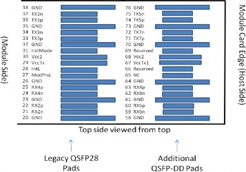
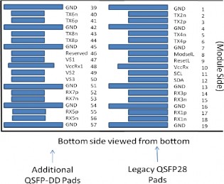
Pin Definition
Pin | Logic | Symbol | Description | Plug Sequence |
1 | GND | Ground | 1B | |
2 | CML-I | Tx2n | Transmitter Inverted Data Input | 3B |
3 | CML-I | Tx2p | Transmitter Non-Inverted Data Input | 3B |
4 | GND | Ground | 1B | |
5 | CML-I | Tx4n | Transmitter Inverted Data Input | 3B |
6 | CML-I | Tx4p | Transmitter Non-Inverted Data Input | 3B |
7 | GND | Ground | 1B | |
8 | LVTTL-I | ModSelL | Module Select | 3B |
9 | LVTTL-I | ResetL | Module Reset | 3B |
10 | VccRx | +3.3V Power Supply Receiver | 2B | |
11 | LVCMOS- I/O | SCL | 2-wire serial interface clock | 3B |
12 | LVCMOS- I/O | SDA | 2-wire serial interface data | 3B |
13 | GND | Ground | 1B | |
14 | CML-O | Rx3p | Receiver Non-Inverted Data Output | 3B |
15 | CML-O | Rx3n | Receiver Inverted Data Output | 3B |
16 | GND | Ground | 1B | |
17 | CML-O | Rx1p | Receiver Non-Inverted Data Output | 3B |
18 | CML-O | Rx1n | Receiver Inverted Data Output | 3B |
19 | GND | Ground | 1B | |
20 | GND | Ground | 1B | |
21 | CML-O | Rx2n | Receiver Inverted Data Output | 3B |
22 | CML-O | Rx2p | Receiver Non-Inverted Data Output | 3B |
23 | GND | Ground | 1B | |
24 | CML-O | Rx4n | Receiver Inverted Data Output | 3B |
25 | CML-O | Rx4p | Receiver Non-Inverted Data Output | 3B |
26 | GND | Ground | 1B | |
27 | LVTTL-O | ModPrsL | Module Present | 3B |
28 | LVTTL-O | IntL | Interrupt | 3B |
29 | VccTx | +3.3V Power supply transmitter | 2B | |
30 | Vcc1 | +3.3V Power supply | 2B | |
31 | LVTTL-I | InitMode | Initialization mode; In legacy QSFP applications, the InitMode pad is called LPMODE | 3B |
32 | GND | Ground | 1B |
33 | CML-I | Tx3p | Transmitter Non-Inverted Data Input | 3B |
34 | CML-I | Tx3n | Transmitter Inverted Data Input | 3B |
35 | GND | Ground | 1B | |
36 | CML-I | Tx1p | Transmitter Non-Inverted Data Input | 3B |
37 | CML-I | Tx1n | Transmitter Inverted Data Input | 3B |
38 | GND | Ground | 1B | |
39 | GND | Ground | 1A | |
40 | CML-I | Tx6n | Transmitter Inverted Data Input | 3A |
41 | CML-I | Tx6p | Transmitter Non-Inverted Data Input | 3A |
42 | GND | Ground | 1A | |
43 | CML-I | Tx8n | Transmitter Inverted Data Input | 3A |
44 | CML-I | Tx8p | Transmitter Non-Inverted Data Input | 3A |
45 | GND | Ground | 1A | |
46 | Reserved | For future use | 3A | |
47 | VS1 | Module Vendor Specific 1 | 3A | |
48 | VccRx1 | 3.3V Power Supply | 2A | |
49 | VS2 | Module Vendor Specific 2 | 3A | |
50 | VS3 | Module Vendor Specific 3 | 3A | |
51 | GND | Ground | 1A | |
52 | CML-O | Rx7p | Receiver Non-Inverted Data Output | 3A |
53 | CML-O | Rx7n | Receiver Inverted Data Output | 3A |
54 | GND | Ground | 1A | |
55 | CML-O | Rx5p | Receiver Non-Inverted Data Output | 3A |
56 | CML-O | Rx5n | Receiver Inverted Data Output | 3A |
57 | GND | Ground | 1A | |
58 | GND | Ground | 1A | |
59 | CML-O | Rx6n | Receiver Inverted Data Output | 3A |
60 | CML-O | Rx6p | Receiver Non-Inverted Data Output | 3A |
61 | GND | Ground | 1A | |
62 | CML-O | Rx8n | Receiver Inverted Data Output | 3A |
63 | CML-O | Rx8p | Receiver Non-Inverted Data Output | 3A |
64 | GND | Ground | 1A | |
65 | NC | No Connect | 3A | |
66 | Reserved | For future use | 3A | |
67 | VccTx1 | 3.3V Power Supply | 2A | |
68 | Vcc2 | 3.3V Power Supply | 2A | |
69 | Reserved | For Future Use | 3A | |
70 | GND | Ground | 1A | |
71 | CML-I | Tx7p | Transmitter Non-Inverted Data Input | 3A |
72 | CML-I | Tx7n | Transmitter Inverted Data Input | 3A |
73 | GND | Ground | 1A | |
74 | CML-I | Tx5p | Transmitter Non-Inverted Data Input | 3A |
75 | CML-I | Tx5n | Transmitter Inverted Data Input | 3A |
76 | GND | Ground | 1A |
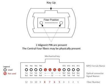
Optical Interface Lanes and Assignment
Figure 3 shows the orientation of the multi-mode fiber facets of the optical connector. Table 1 provides the lane assignment.
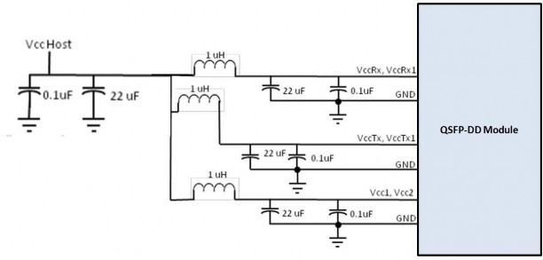
Recommended Power Supply Filter
Absolute Maximum Ratings
It has to be noted that the operation in excess of any individual absolute maximum ratings might cause permanent damage to this module.
Parameter | Symbol | Min | Max | Units | Notes |
Storage Temperature | TS | -40 | 85 | degC | |
Operating Case Temperature - Commercial | TOP | 0 | 70 | degC | |
Operating Case Temperature - Industrial | TOP | -40 | 85 | degC | |
Power Supply Voltage | VCC | -0.5 | 3.6 | V | |
Relative Humidity (non-condensation) | RH | 0 | 85 | % | |
Damage Threshold, each Lane | THd | 3.4 | dBm |
Recommended Operating Conditions and Power Supply Requirements
Parameter | Symbol | Min | Typical | Max | Units | Notes |
Operating Case Temperature | TOP | 0 | 70 | degC | ||
Power Supply Voltage | VCC | 3.135 | 3.3 | 3.465 | V | |
Data Rate, each Lane | 26.5625 | GBd | PAM4 | |||
Data Rate Accuracy | -100 | 100 | ppm | |||
Pre-FEC Bit Error Ratio | 2.4x10⁻⁴ | |||||
Post-FEC Bit Error Ratio | 1x10-12 | 1 | ||||
Link Distance OM3/OM5 | D | 0.5 | 70/150 | m | 2 |
Notes:
FEC provided by host system.
FEC required on host system to support maximum distance.
Electrical Characteristics
The following electrical characteristics are defined over the Recommended Operating Environment unless otherwise specified.
Parameter | Test Point | Min | Typical | Max | Units | Notes |
Power Consumption | 12 | W | ||||
Supply Current | Icc | 3.64 | A | |||
Transmitter (each Lane) | ||||||
Signaling Rate, each Lane | TP1 | 26.5625 ± 100 ppm | GBd | |||
Differential pk-pk Input Voltage Tolerance | TP1a | 900 | mVpp | 1 | ||
Differential Termination Mismatch | TP1 | 10 | % | |||
Differential Input Return Loss | TP1 | IEEE 802.3-2015 Equ. (83E-5) | dB | |||
Differential to Common Mode Input Return Loss | TP1 | IEEE 802.3-2015 Equ. (83E-6) | dB | |||
Module Stressed Input Test | TP1a | See IEEE 802.3bs 120E.3.4.1 | 2 | |||
Single-ended Voltage Tolerance Range (Min) | TP1a | -0.4 to 3.3 | V | |||
DC Common Mode Input Voltage | TP1 | -350 | 2850 | mV | 3 | |
Receiver (each Lane) | ||||||
Signaling Rate, each lane | TP4 | 26.5625 ± 100 ppm | GBd | |||
Differential Peak-to-Peak Output Voltage | TP4 | 900 | mVpp | |||
AC Common Mode Output Voltage, RMS | TP4 | 17.5 | mV | |||
Differential Termination Mismatch | TP4 | 10 | % | |||
Differential Output Return Loss | TP4 | IEEE 802.3-2015 Equ. (83E-2) | ||||
Common to Differential Mode Conversion Return Loss | TP4 | IEEE 802.3-2015 Equ. (83E-3) | ||||
Transition Time, 20% to 80% | TP4 | 9.5 | ps | |||
Near-end Eye Symmetry Mask Width (ESMW) | TP4 | 0.265 | UI | |||
Near-end Eye Height, Differential | TP4 | 70 | mV | |||
Far-end Eye Symmetry Mask Width (ESMW) | TP4 | 0.2 | UI | |||
Far-end Eye Height, Differential | TP4 | 30 | mV | |||
Far-end Pre-cursor ISI Ratio | TP4 | -4.5 | 2.5 | % | ||
Common Mode Output Voltage (Vcm) | TP4 | -350 | 2850 | mV | 3 | |
Notes:
With the exception to IEEE 802.3bs 120E.3.1.2 that the pattern is PRBS31Q or scrambled idle.
Meets BER specified in IEEE 802.3bs 120E.1.1.
DC common mode voltage generated by the host. Specification includes effectsof ground offset voltage.
Optical Characteristics
Parameter | Symbol | Min | Typical | Max | Units | Notes |
Transmitter | ||||||
Center Wavelength | λ1 | 844 | 863 | nm | ||
Center Wavelength | λ2 | 900 | 918 | nm | ||
RMS Spectral Width | ∆λrms | λ 1:0.6 λ2: 0.65 | nm | |||
Average Launch Power, each Lane | PAVG | - 6.5 | 4 | dBm | 1 | |
Optical Modulation Amplitude (OMA), each Lane | POMA | -4.5 | 3 | dBm | 2 | |
Launch power in OMA minus TDECQ, each lane | -5.9 | dBm | ||||
Outer Optical Modulation Amplitude (OMAouter), each Lane | POMA | -0.8 | 4.2 | dBm | 2 | |
Launch Power in OMAouter minus TDECQ, each Lane | -2.2 | dB | ||||
Transmitter Dispersion Penalty,each lane | TDECQ | 4.5 | dB | 3 | ||
TDECQ – 10log10(Ceq ), each lane | 4.5 | 4 | ||||
Extinction Ratio | ER | 3.0 | dB | |||
RIN12 OMA | -128 | dB/Hz | ||||
Optical Return Loss Tolerance | TOL | 12 | dB | |||
Average Launch Power OFF Transmitter, each Lane | Poff | -30 | dBm | |||
Encircled Flux | ≥ 86% at 19 μm ≤ 30% at 4.5 μm | 5 | ||||
Receiver | ||||||
Signaling Rate, each Lane | 26.5625± 100ppm | GBd | ||||
Modulation Format | PAM4 | |||||
Center Wavelength Lane0 | λ1 | 844 | 863 | nm | ||
Center Wavelength Lane1 | λ2 | 900 | 918 | nm | ||
Damage Threshold, each Lane | THd | 5 | dBm | 6 | ||
Average Receive Power, each Lane | -8.5 | 4 | dBm | 7 | ||
Receive Power (OMA), each Lane | 3.0 | dBm | ||||
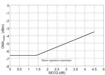
Receiver Sensitivity (OMAouter), each Lane | SEN | Max (- 6.6, SECQ – 8) Refer to Figure 5 | dBm | 9 | ||
Stressed Receiver Sensitivity (OMAouter), each Lane | SRS | -3.5 | dBm | 8 | ||
Receiver Reflectance | RR | -12 | dB |
Notes:
Average launch power, each lane (min) is informative and not the principal indicator of signal strength. A transmitter with launch power below this value cannot be compliant; however, a value above this does not ensure compliance.
Even if the TDECQ < 1.4 dB, the OMAouter (min) must exceed this value.
TDECq is specified and measured as per IEEE802.3.cm Clause 150.8.5.
Ceq is a coefficient defined in IEEE 802.3-2018 Clause 121.8.5.8, which accounts for the reference equalizer noise enhancement.
If measured into type A1a.2, or type A1a.3, or type A1a.4, 50 um fibers in accordance with IEC 61280-1-4.
The receiver shall be able to tolerate, without damage, continuous exposure to an optical input signal having this average power level on one lane. The receiver does not have to operate correctly at this input power.
Average receive power, each lane (min) is informative and not the principal indicator of signal strength. A received power below this value cannot be compliant; however, a value above this does not ensure compliance.
Measured with a conformance test signal at TP3 (see IEEE 802.3 Cl 150 ) for the BER specified. They are not characteristics of the receiver. The conditions for measuring stressed receiver sensitivity are the following:
Stressed eye closure (SECQ), lane under test | 4.5 | dB |
SECQ – 10log10(Ceq) lane under test (max) | 4.5 | dBm |
OMAouter of each aggressor lane | 3.0 | dBm |
These test conditions are for measuring stressed receiver sensitivity.
Receiver sensitivity is considered a normative requirement. RX sensitivity is defined for a transmitter with a value of SECQ up to 4.5dB. For transmitter with SECQ different from 4.5dB, limit is reported as per figure 5
Digital Diagnostic Functions
The following digital diagnostic characteristics are defined over the normal operating conditions unless otherwise specified.
Parameter | Symbol | Min | Max | Units | Notes |
Temperature monitor absolute error | DMI_Temp | -3 | 3 | degC | Over operating temperature range |
Supply voltage monitor absolute error | DMI _VCC | -0.1 | 0.1 | V | Over full operating range |
Channel RX power monitor absolute error | DMI_RX_Ch | -2 | 2 | dB | 1 |
Channel Bias current monitor | DMI_Ibias_Ch | - 10% | 10% | mA | |
Channel TX power monitor absolute error | DMI_TX_Ch | -2 | 2 | dB | 1 |
Notes:
Due to measurement accuracy of different single mode fibers, there could be an additional +/-1 dB fluctuation, or a +/- 3 dB total accuracy.
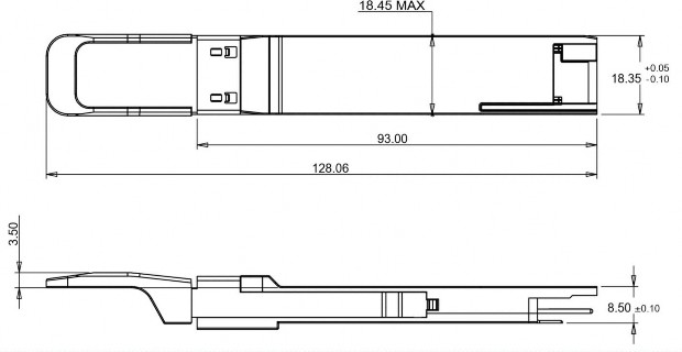
Mechanical Dimensions
ESD
This transceiver is specified as ESD threshold 1kV for high speed data pins and 2kV for all others electrical input pins, tested per MIL-STD-883, Method 3015.4 /JESD22-A114-A (HBM). However, normal ESD precautions are still required during the handling of this module. This transceiver is shipped in ESD protective packaging. It should be removed from the packaging and handled only in an ESD protected environment.
Laser Safety
This is a Class 1M Laser Product according to EN 60825-1:2014. This product complies with 21 CFR 1040.10 except for deviations pursuant to Laser Notice No. 50, dated (June 24, 2007).
Caution: Use of controls or adjustments or performance of procedures other than those specified herein may result in hazardous radiation exposure.
Licensing
The following U.S. patents are licensed by Finisar to FluxLight, Inc.:
U.S. Patent Nos: 7,184,668, 7,079,775, 6,957,021, 7,058,310, 6,952,531, 7,162,160, 7,050,720