
Part Number: QSFP-100G-ER4L-A-FL
QSFP-100G-ER4L-A-EXT-FL QSFP-100G-ER4L-A-IND-FL
Form Factor: QSFP28 TX Wavelength: 1310nm Reach: 40km
Cable Type: SMF Rate Category: 100G
Interface Type: ER4L-A-FL DDM: Yes
Connector Type: Dual-LC
Arista Compatible QSFP-100G-ER4L-A-FL Features
Hot pluggable QSFP28 MSA form factor
Compliant to Ethernet 100GBASE-ER4 Lite and OTN OTU4 4L1-9C1F Lite
Up to 30km reach for G.652 SMF without FEC
Up to 40km reach for G.652 SMF with FEC
Single +3.3V power supply
Transmitter: 4x28Gb/s LAN WDM TOSA (1295.56, 1300.05, 1304.58, 1309.14nm)
Receiver: 4x28Gb/s APD ROSA
Maximum power consumption 4.2W
Duplex LC receptacle
RoHS-6 compliant
Operating Case Temperature
Standard: 0℃ to +70℃
Extended: -5℃ to 85℃
Industrial: -20℃ to +85℃
Arista Compatible QSFP-100G-ER4L-A-FL Applications
100GBASE-ER4 Ethernet Links
OTN OTU4
Product Description
This product is a 100Gb/s transceiver module designed for optical communication applications compliant to Ethernet IEEE 802.3ba standard. The module converts 4 input channels of 28Gb/s electrical data to 4 channels of LAN WDM optical signals and then multiplexes them into a single channel for 100Gb/s optical transmission. Reversely on the receiver side, the module de-multiplexes a 100Gb/s optical input into 4 channels of LAN WDM optical signals and then converts them to 4 output channels of electrical data.
The central wavelengths of the 4 LAN WDM channels are 1295.56, 1300.05, 1304.58 and 1309.14 nm as members of the LAN WDM wavelength grid defined in IEEE 802.3ba standard. The high-performance LAN WDM transmitters and high sensitivity APD receivers provide superior performance for 100Gigabit applications up to 32km links and compliant to optical interface with 100GBASE-ER4 lite requirements.
The product is designed with form factor, optical/electrical connection and digital diagnostic interface according to the QSFP28 Multi-Source Agreement (MSA). It has been designed to meet the harshest external operating conditions including temperature, humidity and EMI interference.
ABSOLUTE MAXIMUM RATINGS
The operation in excess of any absolute maximum ratings might cause permanent damage to this module.
Parameter | Symbol | Min | Max | Unit | Notes |
Storage Temperature | TS | -40 | 85 | degC | |
Operating Case Temperature - Commercial | TOP | 0 | 70 | degC | |
Operating Case Temperature – Extended | TOP | -5 | 85 | degC | |
Operating Case Temperature - Industrial | TOP | -20 | 85 | degC | |
Power Supply Voltage | VCC | -0.5 | 3.6 | V | |
Relative Humidity (non-condensation) | RH | 0 | 85 | % | |
Damage Threshold, each Lane | THd | -3 | dBm |
RECOMMENDED OPERATING CONDITIONS
Parameter | Symbo l | Min | Typical | Max | Unit | Notes |
Operating Case Temperature - Commercial | TOP | 0 | 70 | degC | ||
Operating Case Temperature – Extended | TOP | -5 | 85 | degC | ||
Operating Case Temperature - Industrial | TOP | -20 | 85 | degC | ||
Power Supply Voltage | VCC | 3.135 | 3.3 | 3.465 | V | |
Data Rate, each Lane | 25.78125 | Gb/s | ||||
Control Input Voltage High | 2 | Vcc | V | |||
Control Input Voltage Low | 0 | 0.8 | V | |||
Link Distance with G.652 | D | 0.002 | 40 | km | ||
Operating Case Temperature | TOP | 0 | 70 | degC | ||
Power Supply Voltage | VCC | 3.135 | 3.3 | 3.465 | V |
Electrical Characteristics
Parameter | Test Point | Min | Typical | Max | Unit | Notes |
Power Consumption | 4.2 | W | ||||
Supply Current | Icc | 1.27 | A | |||
Single-ended Input Voltage Tolerance (Note 1) | -0.3 | 4.0 | V | Referred to TP1 signal common | ||
AC Common Mode Input Voltage Tolerance | 15 | mV | RMS | |||
Differential Input Voltage Swing | Vin,pp | 900 | mVpp | |||
Differential Input Impedance | Zin | 90 | 100 | 110 | Ohm | |
Single-ended Output Voltage | -0.3 | 4.0 | V | Referred to signal common | ||
AC Common Mode Output Voltage | 7.5 | mV | RMS | |||
Differential Output Voltage Swing | Vout,pp | 300 | 850 | mVpp | ||
Differential Output Impedance | Zout | 90 | 100 | 110 | Ohm |
1. The single ended input voltage tolerance is the allowable range of the instantaneous input signals.
Optical Characteristics
Parameter | Symbol | Min | Typical | Max | Unit | Notes |
Wavelength Assignment | L0 | 1294.53 | 1295.56 | 1296.59 | nm | |
L1 | 1299.02 | 1300.05 | 1301.09 | nm | ||
L2 | 1303.54 | 1304.58 | 1305.63 | nm | ||
L3 | 1308.09 | 1309.14 | 1310.19 | nm | ||
Transmitter | ||||||
Side Mode Suppression Ratio | SMSR | 30 | dB | |||
Total Average Launch Power | PT | 12.5 | dBm | |||
Average Launch Power, each Lane | PAVG | -2.5 | 6.5 | dBm | ||
OMA, each Lane | POMA | 0.5 | 6.5 | dBm | 1 | |
Difference in Launch Power between any Two Lanes (OMA) | Ptx,diff | 3 | dB | |||
Launch Power in OMA minus Transmitter and Dispersion Penalty (TDP), each Lane | -0.5 | dBm | ||||
TDP, each Lane | TDP | 3.0 | dB | |||
Extinction Ratio | ER | 4.5 | dB | |||
Optical Return Loss Tolerance | TOL | 20 | dB | |||
Transmitter Reflectance | RT | -12 | dB | |||
Eye Mask{X1, X2, X3, Y1, Y2, Y3} | {0.25, 0.4, 0.45, 0.25, 0.28, 0.4} | |||||
Average Launch Power OFF Transmitter, each Lane | Poff | -30 | dBm | |||
Receiver | ||||||
Damage Threshold, each Lane | THd | -6 | dBm | |||
Average Receive Power, each Lane | -20.5 | -7 | dBm | |||
Receive Power (OMA), each Lane | -7 | dBm | ||||
Receiver Sensitivity (OMA, 100GE), each Lane | SEN | -15 | dBm | for BER = 1x10- 12 | ||
Receiver Sensitivity (OMA, 100GE), each Lane | SEN | -18.5 | dBm | For BER = 5x10- 5 | ||
Receiver Sensitivity (OMA, OTU4), each Lane | SEN | -14 | dBm | for BER = 5x10- 12 | ||
Receiver Sensitivity (OMA, OTU4), each Lane | SEN | -18 | dBm | for BER = 5x10⁻⁵ | ||
Difference in Receive Power between any Two Lanes (OMA) | Prx,diff | 3.6 | dB | |||
LOS Assert | LOSA | -26 | dBm | |||
LOS Deassert | LOSD | -24 | dBm | |||
LOS Hysteresis | LOSH | 0.5 | dB | |||
Receiver Electrical 3 dB upper Cutoff Frequency, each Lane | Fc | 31 | GHz | |||
Conditions of Stress Receiver Sensitivity Test (Note 5) | ||||||
Vertical Eye Closure Penalty, each Lane | 2.5 | dB | ||||
Stressed Eye J2 Jitter, each Lane | 0.33 | UI | ||||
Stressed Eye J9 Jitter, each Lane | 0.48 | UI | ||||
1. Even if the TDP < 1 dB, the OMA min must exceed the minimum value specified here.
Digital Diagnostic Functions
The following digital diagnostic characteristics are defined over the normal operating conditions unless otherwise specified.
Parameter | Symbol | Min | Max | Unit | Notes |
Temperature monitor absolute error | DMI_Temp | -3 | 3 | degC | Over operating temp |
Supply voltage monitor absolute error | DMI _VCC | -0.1 | 0.1 | V | Full operating range |
Channel RX power monitor absolute error | DMI_RX | -3 | 3 | dB | Per channel |
Channel Bias current monitor | DMI_Ibias | -10% | 10% | mA | Per channel |
Channel TX power monitor absolute error | DMI_TX | -3 | 3 | dB | Per channel |
PIN Assignment and Description
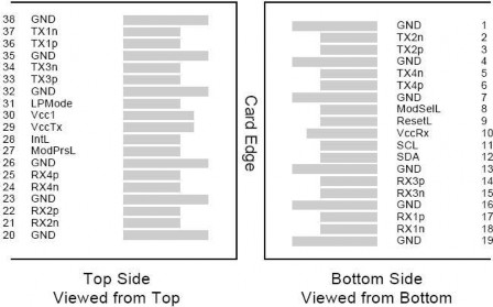
PIN # | Logic | Symbol | Description | Notes |
1 | GND | Ground | ||
2 | CML-I | Tx2n | Transmitter Inverted Data Input | |
3 | CML-I | Tx2p | Transmitter Non-Inverted Data output | |
4 | GND | Ground | ||
5 | CML-I | Tx4n | Transmitter Inverted Data Input | |
6 | CML-I | Tx4p | Transmitter Non-Inverted Data output | |
7 | GND | Ground | ||
8 | LVTLL-I | ModSelL | Module Select | |
9 | LVTLL-I | ResetL | Module Reset | |
10 | VccRx | +3.3V Power Supply Receiver | ||
11 | LVCMOS-I/O | SCL | 2-Wire Serial Interface Clock | |
12 | LVCMOS-I/O | SDA | 2-Wire Serial Interface Data | |
13 | GND | Ground | ||
14 | CML-O | Rx3p | Receiver Non-Inverted Data Output | |
15 | CML-O | Rx3n | Receiver Inverted Data Output | |
16 | GND | Ground | ||
17 | CML-O | Rx1p | Receiver Non-Inverted Data Output | |
18 | CML-O | Rx1n | Receiver Inverted Data Output | |
19 | GND | Ground | ||
20 | GND | Ground | ||
21 | CML-O | Rx2n | Receiver Inverted Data Output | |
22 | CML-O | Rx2p | Receiver Non-Inverted Data Output | |
23 | GND | Ground | ||
24 | CML-O | Rx4n | Receiver Inverted Data Output | |
25 | CML-O | Rx4p | Receiver Non-Inverted Data Output | |
26 | GND | Ground | ||
27 | LVTTL-O | ModPrsL | Module Present | |
28 | LVTTL-O | IntL | Interrupt | |
29 | VccTx | +3.3 V Power Supply transmitter | ||
30 | Vcc1 | +3.3 V Power Supply | ||
31 | LVTTL-I | LPMode | Low Power Mode | |
32 | GND | Ground | ||
33 | CML-I | Tx3p | Transmitter Non-Inverted Data Input | |
34 | CML-I | Tx3n | Transmitter Inverted Data Output | |
35 | GND | Ground | ||
36 | CML-I | Tx1p | Transmitter Non-Inverted Data Input | |
37 | CML-I | Tx1n | Transmitter Inverted Data Output | |
38 | GND | Ground |
Mechanical Dimension
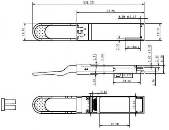
(Unit: mm)
ESD
This transceiver is specified as ESD threshold 1kV for SFI APDs and 2kV for all other electrical input APDs, tested per MIL- STD-883, Method 3015.4 /JESD22-A114-A (HBM). However, normal ESD precautions are still required during the handling of this module. This transceiver is shipped in ESD protective packaging. It should be removed from the packaging and handled only in an ESD protected environment.
Laser Safety
This is a Class 1 Laser Product according to IEC 60825-1:2007. This product complies with 21 CFR 1040.10 and 1040.11 except for deviations pursuant to Laser Notice No. 50, dated (June 24, 2007).
Licensing
The following U.S. patents are licensed by Finisar to FluxLight, Inc.:
U.S. Patent Nos: 7,184,668, 7,079,775, 6,957,021, 7,058,310, 6,952,531, 7,162,160, 7,050,720