
Quick Spec:
Part Number: QSFP28-100G-FR QSFP28-100G-FR-EXT QSFP28-100G-FR-IND
Form Factor: QSFP28
TX Wavelength: 1310nm
Reach: 2km
Cable Type: SMF
Rate Category: 100GBase
Interface Type: FR4
DDM: Yes
Connector Type: Dual-LC
Features
Qsfp28 MSA complaint
Support 53.125Gbaud
100G Lambda MSA 100G-FR Specification compliant
Up to 2km transmission on single mode fiber(SMF) with FEC
Operating case temperature: 0 to 70oC
4x25G electrical interface (OIF CEI-28G-VSR)
Maximum power consumption 4.5W
LC duplex connector
RoHS compliant
Operating Case Temperature
Standard: 0°C to +70 °C
Extended -5°C to +85 °C
Industrial -40°C to +85 °C
Applications
Data Center Interconnect
100G Ethernet
Enterprise networking
Absolute Maximum Ratings
Parameter | Symbol | Min. | Max. | Units | Note |
Storage Temperature | Ts | -40 | 85 | ℃ | |
Operating Case Temperature | TOP | 0 | 70 | ℃ | |
Supply Voltage | VCC | -0.5 | 3.6 | V | |
Relative Humidity (non-condensation) | RH | 0 | 85 | % | |
Damage Threshold, each Lane | THd | 5.5 | dBm |
Recommended Operating Conditions
Parameter | Symbol | Min. | Typ. | Max. | Units | Notes |
Operating Case Temperature | TOP | 0 | 70 | ℃ | ||
Power Supply Voltage | Vcc | 3.135 | 3.3 | 3.465 | V | |
Data Rate,each Lane | 25.78125 | Gb/s | ||||
Optical Data Rate(PAM4) | 53.125 | GBd | ||||
Data Rate Accuracy | -100 | 100 | ppm | |||
Pre-FEC Bit Error Ratio | 2.4x10⁻⁴ | |||||
Post-FEC Bit Error Ratio | 1x10-12 | 1 | ||||
Control Input Voltage High | 2 | Vcc | V | |||
Control Input Voltage Low | 0 | 0.8 | V | |||
LinkDistancewithG.652 | D | 0.002 | 2 | km | 2 |
Notes:
FEC feature is embedded in the module.
FEC required to be turned on to support maximum transmission distance.
Diagnostics Monitoring
Parameter | Symbol | Accuracy | Units | Notes |
Temperature monitor absolute Error | DMI_Temp | ± 3 | Over operataing temperature range | |
Supply voltage monitor absolute error | DMI_VCC | ± 0.1 | V | Over full operating range |
Channel RX power monitor absolute error | DMI_RX_Ch | ± 2 | dB | 1 |
Channel Bias Current | DMI_Ibias_Ch | ± 10% | mA | |
Channel TX power monitor absolute error | DMI_TX_Ch | ± 2 | Db | 1 |
Notes:
1. Due to measurement accuracy of different single mode fibers, there could be an additional +/-1 dB fluctuation, or a +/- 3 dB total accuracy.
Transmitter Electro-optical Characteristics (Each Lane)
Parameter | Test Point | Min | Typ. | Max | Units | Notes |
Power Consumption | 4.5 | W | ||||
Supply Current | Icc | 1.36 | A | |||
Overload Differential Voltage pk-pk | TP1a | 900 | mV | |||
Common Mode Voltage (Vcm) | TP1 | -350 | 2850 | mV | 1 | |
Differential Termination Resistance Mismatch | TP1 | 10 | % | At 1MHz | ||
Differential Return Loss (SDD11) | TP1 | See CEI- 28G-VSR Equation 13- 19 | dB | |||
Common Mode to Differential conversion and Differential to Common Mode conversion (SDC11, SCD11) | TP1 | See CEI- 28G-VSR Equation 13-21 | dB | |||
Center Wavelength | Λt | 1304.5 | 1317.5 | nm | ||
Side Mode Suppression Ratio | SMSR | 30 | dB | |||
Launch Power, each Lane | PAVG | -2.4 | 4 | dBm | 1 | |
Outer Optical Modulation Amplitude (OMAouter) | POMA | -0.2 | 4.2 | dBm | 2 | |
Launch Power in OMA minus TDECQ For ER ≧4.5dB For ER < 4.5dB | -1.6 -1.5 | dBm |
Transmitter and Dispersion Eye Closure for PAM4 (TDECQ) | TDECQ | 3.4 | dB | |||
TDECQ-10*log10 (Ceq) | 3.4 | dB | 3 | |||
Extinction Ratio | ER | 3.5 | dB | |||
RIN17.1 OMA | RIN | -136 | dB/Hz | |||
Optical Return Loss Tolerance | TOL | 17.1 | dB | |||
Transmitter Reflectance | RT | -26 | dB | |||
Transmitter Transition Time | 17 | ps | ||||
Average Launch Power OFF Transmitter, each Lane | Poff | -15 | dBm | |||
Receiver Electro-Optical Characteristics (each Lane)
Parameter | Test Point | Min | Max | Units | Notes |
Differential Voltage, pk-pk | TP4 | 900 | mV | ||
Common Mode Voltage (Vcm) | TP4 | -350 | 2850 | mV | 1 |
Common Mode Noise, RMS | TP4 | 17.5 | mV | ||
Differential Termination Resistance Mismatch | TP4 | 10 | % | At 1MHZ | |
Differential bReturn Loss (SDD22) | TP4 | See CEI-28G- VSR, Equation 13- 19 | dB | ||
Common Mode to Differential Conversion and Differential to Common Mode Conversion (SDC22, SCD22) | TP4 | See CEI-28G- VSR, Equation 13- 21 | dB | ||
Transition Time, 20% to 80% | TP4 | 9.5 | ps | ||
Common Mode Return Loss (SCC22) | TP4 | -2 | dB | 2 | |
Vertical Eye Closure (VEC) | TP4 | 5.5 | dB | ||
Eye Width at 10-15 probability (EW15) | TP4 | 0.57 | UI | ||
Eye Height at 10-15 probability (EH15) | TP4 | 228 | mV | ||
Center Wavelength | Λr | 1305 | 1317.5 | Nm | |
Damage Threshold | THd | 5.5 | dBm | 4 | |
Average Receive Power | -6.4 | 4.5 | dBm | 5 | |
Receive Power (OMAouter) | 4.7 | dBm | |||
Receiver Sensitivity (OMAouter) | SEN | Equation (1) | dBm | 6 | |
Stressed Receiver Sensitivity (OMAouter) | SRS | -2.5 | dBm | 7 | |
Receiver Reflectance | RR | -26 | dB |
LOS Assert | LOSA | 15 | dBm | ||
LOS Deassert | LOSD | -9.4 | dBm | ||
LOS Hysteresis | LOSH | 0.5 | dB | ||
Stressed Eye Closure fo rPAM4 | 3.4 | dB | |||
SECQ-10*log10(Ceq) | 3.4 | dB |
Notes:
Average launch power, each lane min is informative and not the principal indicator of signal strength. A transmitter with launch power below this value cannot be compliant, however, a value above this does not ensure compliance.
Even if the TDECQ < 1.4 dB for an extinction ratio of ≧4.5dB or TDECQ < 1.3dB for an extinction ratio of <4.5dB, the OMAouter (min) must exceed the minimum value specified here.
Ceq is a coefficient defined in IEEE Std 802.3-2018 clause 121.8.5.3 which accounts for reference equalizer noise
enhancement.
Average receiver power (min) is informative and not the principal indicator of signal strength. A received powerbelow this value cannot be compliant, however, a value above this does not ensure compliance.
The receiver shall be able to tolerate, without damage, continuous exposure to a modulated optical input signal having this power level on one lane. The receiver does not have to operate correctly at this input power.
Receiver sensitivity (OMAouter) (max) is informative and is defined for a transmitter with a value of SECQ upto 3.4dB. It should meet Equation (1), which is illustrated in Figure 4.
Measured with conformance test signal at TP3 for the BER equal to 2.4x10⁻⁴
The test conditions are for measuring stressed receiver sensitivity. They are not characteristics of the receiver.

Block Diagram of Transceiver

This product is a transceiver module designed for 2km optical communication applications. The module incorporates one channel optical signal, on 1310nm center wavelength, operating at 50Gbaud data rate. The transmitter path incorporates an EML Driver and a cooled EML together. On the receiver path, the inpirt optical signal is coupled to a Pin photodiode detector. A DSP based gearbox is used to convert 4x25Gbps NRZ signals to 1x50Gbaud PAM4 signal. Also a 4-channel retimer and FEC block are integrated in this DSP. The electrical interface is compliant with IEEE 802.3cd and QSFP28 MSA in the transmitting and receiving directions, and optical interface is compliant to IEEE 802.3cd and 100G Lambda MSA with Duplex LC connector The module has a maximum power consumption of 4.5W.
The product is designed with form factor, optical/electrical connection and digital diagnostic interface according to the QSFP28 Multi-Source Agreement (MSA). It has been designed to meet the harshest external operating conditions including temperature, humidity and EMI interference.
This product converts the 4-channel 100Gb/s aggregated NRZ electrical input data into one channel of 50Gbaud PAM4 optical signal (light) on 1310nm center wavelength through a DSP based gearbox, by a driven cooled Electro-absorption Modulated DFB Laser (EML). The light propagates out of the transmitter into an SMFfiber. The receiver module accepts the 50Gbaud PAM4 optical signal input, and converts it into a 50Gbaud PAM4 electrical signal via a linear amplifier. And then convert the 5Gbaud PAM4 signal into 4 channels of 25Gbps NRZ signals. Figure 1 shows the functional block diagram of this product.
A single +3.3V power supply is required to power up this product. Both power supply pins VccTx and VccRx are internally connected and should be applied concurrently. As per MSA specifications the module offers 7 lowspeed hardware control pins (including the 2-wire serial interface): ModSelL, SCL, SDA, ResetL, LPMode, ModPrsL and IntL.
Module Select (ModSelL) is an input pin. When held low by the host, this product responds to 2-wire serial communication commands. The ModSelL allows the use of this product on a single 2-wire interface bus – individual ModSelL lines must be used.
Serial Clock (SCL) and Serial Data (SDA) are required for the 2-wire serial bus communication interface and enable the host to access the memory map.
The ResetL pin enables a complete reset, returning the settings to their default state, when a low level on the ResetL pin is held for longer than the minimum pulse length. During the execution of a reset the host shall disregard all status bits until it indicates a completion of the reset interrupt. The product indicates this by postingan IntL (Interrupt) signal with the Data_Not_Ready bit negated in the memory map. Note that on power up (including hot insertion) the module should post this completion of reset interrupt without requiring a reset.
Low Power Mode (LPMode) pin is used to set the maximum power consumption for the product in order to protect hosts that are not capable of cooling higher power modules, should such modules be accidentally inserted
Module Present (ModPrsL) is a signal local to the host board which, in the absence of a product, is normally pulled up to the host Vcc. When the product is inserted into the connector, it completes the path to ground through a resistor on the host board and asserts the signal. ModPrsL then indicates its present by setting ModPrsL to a “Low” state.
Interrupt (IntL) is an output pin. “Low” indicates a possible operational fault or a status critical to the host system. The host identifies the source of the interrupt using the 2-wire serial interface. The IntL pin is an opencollector output and must be pulled to the Host Vcc voltage on the Host board.
Pin Assignment

Pin Description
PIN | Logic | Symbol Name/Description Note | ||
1 | GND | Ground | 1 | |
2 | CML-I | Tx2n | Transmitter Inverted Data Input | |
3 | CML-I | Tx2p | Transmitter Non-Inverted Data output | |
4 | GND | Ground | 1 | |
5 | CML-I | Tx4n | Transmitter inverted Data Input | |
6 | CML-I | Tx4p | Transmitter Non-Inverted Data output | |
7 | GND | Ground | 1 | |
8 | LVTLL-I | ModSeIL | Module Select | |
9 | LVTLL-I | ResetL | Module Reset | |
10 | VccRx | +3.3V Power Supply Receiver | 2 | |
11 | LVCMOS-I/O | SCL | 2-Wire Serial Interface Clock | |
12 | LVCMOS-I/O | SDA | 2-Wire Serial Interface Data | |
13 | GND | Ground | ||
14 | CML-O | Rx3p | Receiver Non-Inverted Data output | |
15 | CML-O | Rx3n | Receiver Inverted Data output | |
16 | GND | Ground | 1 | |
17 | CML-O | Rx1p | Receiver Non-Inverted Data Output | |
18 | CML-O | Rx1n | Receiver Inverted Data Output | |
19 | GND | Ground | 1 | |
20 | GND | Ground | 1 | |
21 | CML-O | Rx2n | Receiver Inverted Data output | |
22 | CML-O | Rx2p | Receiver Non-Inverted Data output | |
23 | GND | Ground | 1 | |
24 | CML-O | Rx4n | Receiver Inverted Data output | 1 |
25 | CML-O | Rx4p | Receiver Non-Inverted Data output | |
26 | GND | Ground | 1 | |
27 | LVTTL-O | ModPrsL | Module Present | |
28 | LVTTL-O | IntL | Interrupt | |
29 | VccTx | +3.3V Power Supply transmitter | 2 | |
30 | Vcc1 | +3.3V Power Supply | 2 | |
31 | LVTTL-I | LPMode | Low Power Mode | |
32 | GND | Ground | 1 | |
33 | CML-I | Tx3p | Transmitter Non-Inverted Data Input | |
34 | CML-I | Tx3n | Transmitter Inverted Data Output | |
35 | GND | Ground | 1 | |
36 | CML-I | Tx1p | Transmitter Non-Inverted Data Input | |
37 | CML-I | Tx1n | Transmitter Inverted Data Output | |
38 | GND | Ground | 1 |
Note:
GND is the symbol for signal and supply (power) common for QSFP28 modules. All are common within theQSFP28 module and all module voltages are referenced to this potential unless otherwise noted. Connect these directly to the host board signal common ground plane.
VccRx, Vcc1 and VccTx are the receiving and transmission power suppliers and shall be applied concurrently. Vcc Rx, Vcc1 and Vcc Tx may be internally connected within the QSFP28 transceiver modulein any combination. The connector pins are each rated for a maximum current of 1000mA.
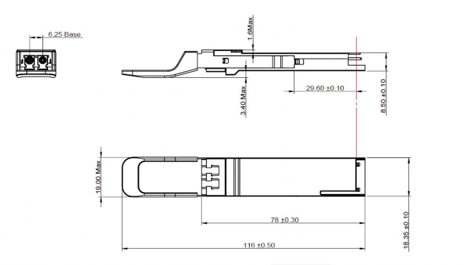
Dimensions
Laser Safety
This is a Class 1 Laser Product according to EN 60825-1:2014. This product complies with 21 CFR 1040.10 and 1040.11 except for deviations pursuant to Laser Notice No. 50, dated (June 24, 2007).
Caution: Use of controls or adjustments or performance of procedures other than those specified herein may result in hazardous radiation exposure.
Licensing
The following U.S. patents are licensed by Finisar to FluxLight, Inc.:
U.S. Patent Nos: 7,184,668, 7,079,775, 6,957,021, 7,058,310, 6,952,531, 7,162,160, 7,050,720